ZHCSIH9F March   2009  – July 2018 TPS65023-Q1

PRODUCTION DATA.  

  1. 特性
  2. 应用
  3. 说明
    1.     Device Images
      1.      简化原理图
  4. 修订历史记录
  5. 说明 (续)
  6. Pin Configuration and Functions
    1.     Pin Functions
  7. Specifications
    1. 7.1 Absolute Maximum Ratings
    2. 7.2 ESD Ratings
    3. 7.3 Recommended Operating Conditions
    4. 7.4 Thermal Information
    5. 7.5 Electrical Characteristics
    6. 7.6 Timing Requirements
    7. 7.7 Typical Characteristics
  8. Detailed Description
    1. 8.1 Overview
    2. 8.2 Functional Block Diagram
    3. 8.3 Feature Description
      1. 8.3.1 Step-Down Converters, VDCDC1, VDCDC2, and VDCDC3
      2. 8.3.2 Soft Start
      3. 8.3.3 Active Discharge When Disabled
      4. 8.3.4 Power-Good Monitoring
      5. 8.3.5 Low-Dropout Voltage Regulators
      6. 8.3.6 Undervoltage Lockout
    4. 8.4 Device Functional Modes
      1. 8.4.1 VRTC Output and Operation With or Without Backup Battery
      2. 8.4.2 Power-Save Mode Operation (PSM)
      3. 8.4.3 Low-Ripple Mode
      4. 8.4.4 100% Duty-Cycle Low-Dropout Operation
      5. 8.4.5 System Reset and Control Signals
        1. 8.4.5.1 DEFLDO1 and DEFLDO2
        2. 8.4.5.2 Interrupt Management and the INT Pin
    5. 8.5 Programming
      1. 8.5.1 Power-Up Sequencing
      2. 8.5.2 Serial Interface
    6. 8.6 Register Maps
      1. 8.6.1 VERSION Register (address: 00h) Read-Only
      2. 8.6.2 PGOODZ Register (address: 01h) Read-Only
        1. Table 5. PGOODZ Register Field Descriptions
      3. 8.6.3 MASK Register (address: 02h)
      4. 8.6.4 REG_CTRL Register (address: 03h)
        1. Table 6. REG_CTRL Register Field Descriptions
      5. 8.6.5 CON_CTRL Register (address: 04h)
        1. Table 7. CON_CTRL Register Field Descriptions
      6. 8.6.6 CON_CTRL2 Register (address: 05h)
        1. Table 8. CON_CTRL2 Register Field Descriptions
      7. 8.6.7 DEFCORE Register (address: 06h)
        1. Table 9. DEFCORE Register Field Descriptions
      8. 8.6.8 DEFSLEW Register (address: 07h)
        1. Table 10. DEFSLEW Register Field Descriptions
      9. 8.6.9 LDO_CTRL Register (address: 08h)
        1. Table 11. LDO_CTRL Register Field Descriptions
  9. Application and Implementation
    1. 9.1 Application Information
      1. 9.1.1 Reset Condition of DCDC1
    2. 9.2 Typical Application
      1. 9.2.1 Design Requirements
      2. 9.2.2 Detailed Design Procedure
        1. 9.2.2.1 Inductor Selection for the DC-DC Converters
        2. 9.2.2.2 Output Capacitor Selection
        3. 9.2.2.3 Input Capacitor Selection
        4. 9.2.2.4 Output Voltage Selection
        5. 9.2.2.5 VRTC Output
        6. 9.2.2.6 LDO1 and LDO2
        7. 9.2.2.7 TRESPWRON
        8. 9.2.2.8 VCC Filter
      3. 9.2.3 Application Curves
  10. 10Power Supply Recommendations
  11. 11Layout
    1. 11.1 Layout Guidelines
    2. 11.2 Layout Example
  12. 12器件和文档支持
    1. 12.1 器件支持
      1. 12.1.1 第三方产品免责声明
    2. 12.2 文档支持
      1. 12.2.1 相关文档
    3. 12.3 接收文档更新通知
    4. 12.4 社区资源
    5. 12.5 商标
    6. 12.6 静电放电警告
    7. 12.7 术语表
  13. 13机械、封装和可订购信息

封装选项

机械数据 (封装 | 引脚)
散热焊盘机械数据 (封装 | 引脚)
订购信息

Reset Condition of DCDC1

If DEFDCDC1 is connected to ground and DCDC1_EN is pulled high after VINDCDC1 is applied, the output voltage of DCDC1 defaults to 1.225 V instead of 1.2 V (high by 2%). Figure 42 illustrates the problem.

TPS65023-Q1 dcdc1_lvs927.gifFigure 42. Default DCDC1

Workaround 1: Tie DCDC1_EN to VINDCDC1 (Figure 43)

TPS65023-Q1 wrkarond1_lvs927.gifFigure 43. Workaround 1

Workaround 2: Write the correct voltage to the DEF_CORE register through I2C. This can be done before or after the converter is enabled. If written before the enable, the only bit changed is DEF_CORE[0]. The voltage is 1.2 V, however, when the enable is pulled high (Figure 44).
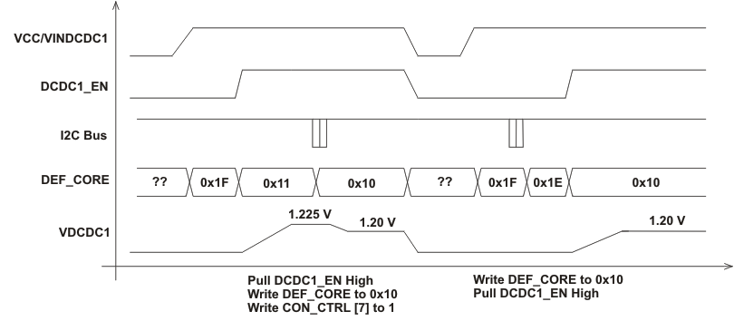
TPS65023-Q1 wrkarond2_lvs927.gifFigure 44. Workaround 2

Workaround 3: Generate a HOT_RESET after enabling DCDC1 (Figure 45)

TPS65023-Q1 wrkarond3_lvs927.gifFigure 45. Workaround 3