SLVS530D SEPTEMBER 2005 – October 2015 TPS63700
PRODUCTION DATA.
- 1 Features
- 2 Applications
- 3 Description
- 4 Revision History
- 5 Pin Configuration and Functions
- 6 Specifications
- 7 Detailed Description
- 8 Application and Implementation
- 9 Power Supply Recommendations
- 10Layout
- 11Device and Documentation Support
- 12Mechanical, Packaging, and Orderable Information
10 Layout
10.1 Layout Guidelines
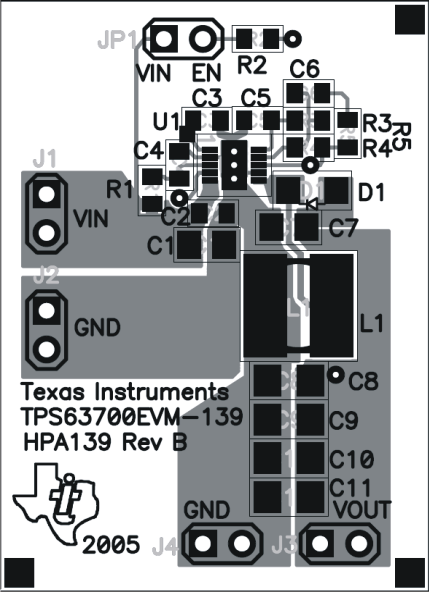
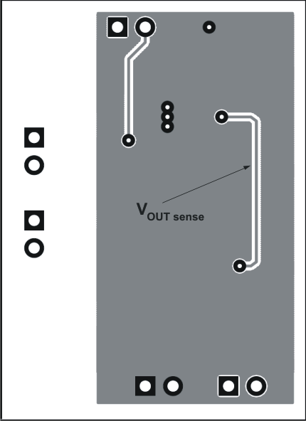
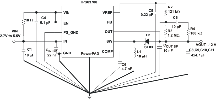
For all switching power supplies the layout is an important step in the design, especially at high peak currents and high switching frequencies. If the layout is not carefully done, the regulator could show stability problems as well as EMI problems. Therefore, use wide and short traces for the main current paths, and for the power-ground tracks. The input and output capacitors should be placed as close as possible to the IC. The diode need to be connected closest to the SW pin to minimize parasitic inductance. For low noise operation small bypass capacitors CIN BP and COUT BP in the nF range can be added close to the IC.
The feedback divider should be placed as close as possible to the VREF pin of the IC. Use short traces when laying out the control ground. Figure 18 shows the layout of the EVM board.
10.2 Layout Example
 Figure 16. Layout Considerations, Top View
 Figure 17. Layout Considerations, Bottom View
 Figure 18. Layout Circuit