SLVS530D SEPTEMBER 2005 – October 2015 TPS63700
PRODUCTION DATA.
- 1 Features
- 2 Applications
- 3 Description
- 4 Revision History
- 5 Pin Configuration and Functions
- 6 Specifications
- 7 Detailed Description
- 8 Application and Implementation
- 9 Power Supply Recommendations
- 10Layout
- 11Device and Documentation Support
- 12Mechanical, Packaging, and Orderable Information
7 Detailed Description
7.1 Overview
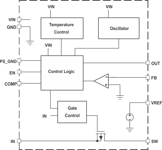
The TPS63700 is a DC/DC converter for negative output voltages using buck-boost topology. It operates with an input voltage range of 2.7 V to 5.5 V and generates a negative output voltage down to –15 V. The output is controlled by a fixed-frequency, pulse-width-modulated (PWM) regulator. In normal operation mode, the converter operates at continuous conduction mode (CCM). At light loads it can enter discontinuous conduction mode (DCM).
7.2 Functional Block Diagram

7.3 Feature Description
7.3.1 Enable
Applying GND signal at the EN pin disables the converter, where all internal circuitry is turned off. The device now just consumes low shutdown current flowing into the VIN pin. The output load of the converter is also disconnected from the battery as described in Load Disconnect. Pulling the EN pin to VIN enables the converter. Internal circuitry, necessary to operate the converter, is then turned on.
7.3.2 Load Disconnect
The device supports complete load disconnection when the converter is disabled. The converter turns off the internal PMOS switch, thus no DC current path remains between load and input voltage source.
7.3.3 Output Overvoltage Protection
The converter has an output overvoltage protection implemented. The output voltage is limited to –19 V in case the feedback connection from the output to the FB pin is open.
7.3.4 Undervoltage Lockout
An undervoltage lockout prevents the device from starting up and operating if the supply voltage at VIN is lower than the programmed threshold shown in the Electrical Characteristics table. The device automatically shuts down the converter when the supply voltage at VIN falls below this threshold. Nevertheless, parts of the control circuits remain active, which is different than device shutdown using EN inputs. The undervoltage lockout function is implemented to prevent device malfunction.
7.3.5 Overtemperature Shutdown
The device automatically shuts down if the implemented internal temperature detector detects a chip temperature above the programmed threshold shown in the electrical characteristics table. It starts operating again when the chip temperature decreases. A built-in temperature hysteresis avoids undefined operation caused by ringing from over-temperature shutdown.
7.4 Device Functional Modes
7.4.1 Soft-Start
The converter has a soft-start function. When the converter is enabled, the implemented switch current limit ramps up slowly to its nominal value. Soft-start is implemented to limit the input current during start-up to avoid high peak currents at the battery which could interfere with other systems connected to the same battery.
Without soft-start, uncontrolled input peak currents flow to charge up the output capacitors and to supply the load during start-up. This would cause significant voltage drops across the series resistance of the battery and its connections.
7.4.2 PWM Operation
The converter operates in a fixed-frequency, pulse-width-modulated control scheme. The on-time of the switches varies depending on input-to-output voltage ratio and the load. During this on-time, the inductor connected to the converter is charged with current. In the remaining time, the time period set by the fixed operating frequency, the inductor discharges into the output capacitor via the rectifier diode. At medium to heavy loads the inductor current is continuous and the device operates in continuous conduction mode (CCM).
7.4.3 Power Save Mode Operation
As the load current decreases, the converter enters Power Save Mode. Entering Power Save Mode happens at the boundary to discontinuous conduction mode (DCM). During light load, the inductor current of this converter can become discontinuous. In this case, the control circuit of the controller output automatically takes care of these changing conditions to always operate with an optimum control setup.
7.4.4 Control
The controller circuit of the converter is based on a fixed-frequency, multiple-feed-forward controller topology. Input voltage, output voltage, and voltage drop across the switch are monitored and forwarded to the regulator. Changes in the operating conditions of the converter directly affect the duty cycle.
The error amplifier compares the voltage at FB pin with GND to generate an accurate and stable output voltage. The error amplifier is internally compensated. At light loads, the converter operates in discontinuous conduction mode (DCM).
If the load will be further decreased, the energy transmitted to the output capacitor cannot be absorbed by the load and would lead to an increase of the output voltage. In this case, the converter limits the output voltage increase by skipping switch pulses.