SLVSAN3B December 2010 – November 2016 TPS61199
PRODUCTION DATA.
- 1 Features
- 2 Applications
- 3 Description
- 4 Revision History
- 5 Pin Configuration and Functions
- 6 Specifications
- 7 Detailed Description
- 8 Application and Implementation
- 9 Power Supply Recommendations
- 10Layout
- 11Device and Documentation Support
- 12Mechanical, Packaging, and Orderable Information
封装选项
机械数据 (封装 | 引脚)
散热焊盘机械数据 (封装 | 引脚)
- PWP|20
订购信息
6 Specifications
6.1 Absolute Maximum Ratings
over operating free-air temperature range (unless otherwise noted)(1)| MIN | MAX | UNIT | ||
|---|---|---|---|---|
| Voltage | Pin VIN(2) | –0.3 | 33 | V |
| Pin IFB1 to IFB8(2) | –0.3 | 30 | ||
| Pin EN and PWM(2) | –0.3 | 20 | ||
| Pin ISET, ISNS and OVP(2) | –0.3 | 3.6 | ||
| All other pins(2) | –0.3 | 7 | ||
| Continuous power dissipation | SeeThermal Information | |||
| Operating junction temperature | –40 | 150 | °C | |
| Storage temperature, Tstg | –65 | 50 | °C | |
(1) Stresses beyond those listed under Absolute Maximum Ratings may cause permanent damage to the device. These are stress ratings only, which do not imply functional operation of the device at these or any other conditions beyond those indicated under Recommended Operating Conditions. Exposure to absolute-maximum-rated conditions for extended periods may affect device reliability.
(2) All voltage values are with respect to network ground terminal
6.2 ESD Ratings
| VALUE | UNIT | |||
|---|---|---|---|---|
| V(ESD) | Electrostatic discharge | Human-body model (HBM), per ANSI/ESDA/JEDEC JS-001(1) | ±2000 | V |
(1) JEDEC document JEP155 states that 500-V HBM allows safe manufacturing with a standard ESD control procedures.
6.3 Recommended Operating Conditions
over operating free-air temperature range (unless otherwise noted)(1)| MIN | NOM | MAX | UNIT | ||
|---|---|---|---|---|---|
| Inductor, L1 | 10 | 22 | 47 | µH | |
| Input capacitor, C1 | 10 | µF | |||
| Output capacitor, C2 | 10 | 33 | 100 | µF | |
| PWM dimming frequency, ƒPWM | 0.1 | 22 | KHz | ||
| Rising/falling edge of PWM signal, tPWM | 1 | µsec | |||
| Boost regulator switching frequency, fBOOST | 300 | 800 | kHz | ||
| Operating ambient temperature, TA | –40 | 85 | °C | ||
(1) Customers must verify the component values in their application if the values are different from the recommended values.
6.4 Thermal Information
| THERMAL METRIC(1) | TPS61199 | TPS61199 | UNITS | |
|---|---|---|---|---|
| NS (SO) | PWP (HTSSOP) | |||
| 20 PINS | 20 PINS | |||
| RθJA | Junction-to-ambient thermal resistance | 69.4 | 46.9 | °C/W |
| RθJC(top) | Junction-to-case (top) thermal resistance | 36.4 | 48.2 | °C/W |
| RθJB | Junction-to-board thermal resistance | 37.3 | 22.1 | °C/W |
| ψJT | Junction-to-top characterization parameter | 11.0 | 3.4 | °C/W |
| ψJB | Junction-to-board characterization parameter | 36.8 | 13.3 | °C/W |
| RθJC(bot) | Junction-to-case (bottom) thermal resistance | n/a | 2.3 | °C/W |
(1) For more information about traditional and new thermal metrics, see Semiconductor and IC Package Thermal Metrics.
6.5 Electrical Characteristics
VIN = 12 V; TA = –40°C to +85°C, typical values are at TA = 25°C (unless otherwise noted)| PARAMETER | TEST CONDITIONS | MIN | TYP | MAX | UNIT | |
|---|---|---|---|---|---|---|
| SUPPLY CURRENT | ||||||
| VIN | Input voltage range | 8 | 30 | V | ||
| VUVLO_VIN | Undervoltage lockout threshold | VIN falling | 6.5 | 7 | V | |
| VVIN_SYS | VIN hysteresis | VIN rising | 300 | mV | ||
| IQ_VIN | Operating quiescent current into VIN | EN = high; PWM = low; no switching, VIN = 30 V |
1.5 | mA | ||
| ISD | Shutdown current | 10 | µA | |||
| VDD | Internal regulation voltage | Output current of VDD = 15 mA | 5.7 | 6 | 6.3 | V |
| EN and PWM | ||||||
| VH | Logic high threshold on EN, PWM | VIN = 8 V to 30 V | 2 | V | ||
| VL | Logic low threshold on EN, PWM | VIN = 8 V to 30 V | 0.8 | V | ||
| RPD | Pulldown resistor on EN, PWM | 400 | 800 | 1600 | kΩ | |
| CURRENT REGULATION | ||||||
| VISET | ISET pin voltage | 1.204 | 1.229 | 1.253 | V | |
| KISET | Current multiple IIFB(AVG) / ISET | IISET = 30 µA; IFB = 450 mV | 1990 | |||
| IFB | Current accuracy to IIFB(AVG) | IISET = 30 µA; IFB = 450 mV | –2% | 2% | ||
| IFB(BR)(1) | Current matching | IISET= 30 µA; IFB = 450 mV | 3% | |||
| IFBleak | IFB pin leakage current | IFB voltage = 30 V; PWM = low | 10 | 25 | 45 | µA |
| IIFB_max | Current sink max output current | IFB = 450 mV | 70 | mA | ||
| OSCILLATOR | ||||||
| ƒOSC | Switching frequency | R = 100 kΩ | 0.66 | 0.8 | 0.94 | MHz |
| R = 160 kΩ | 0.44 | 0.5 | 0.56 | |||
| VFSW | FSW pin reference voltage | 1.229 | V | |||
| Dutymax | Maximum duty cycle | FSW = 500 kHz | 90% | 94% | ||
| tskip | Minimum pulse width for skip cycle mode | 200 | ns | |||
| GATE DRIVER and OVERCURRENT LIMIT | ||||||
| RGDRV(SRC) | Gate driver impedance when sourcing | VGDRV = 6 V, IGDRV = 20 mA | 2 | Ω | ||
| RGDRV(SNK) | Gate driver impedance when sinking | VGDRV = 6 V, IGDRV = 20 mA | 1.5 | Ω | ||
| VISNS | Switch current limit detection threshold | VIN = 8 V to 30 V | 120 | 160 | 180 | mV |
| PROTECTION | ||||||
| VCLAMP | Output overvoltage threshold at OVP pin | 2.77 | 2.95 | 3.13 | V | |
| IFBP | LED short across protection bias current multiple IFBP/IISET | VFBP = 1 V | 0.23 | 0.25 | 0.27 | |
| VOVP_IFB | IFB overvoltage threshold | 26.5 | 29.5 | V | ||
| THERMAL SHUTDOWN | ||||||
| Tshutdown | Thermal shutdown threshold | 150 | °C | |||
(1) Current matching = (IMAX – IMIN) / IAVG
6.6 Typical Characteristics
Typical Application as test circuit, and L = CDRH127/HPNP- 220M, R6 = 41kΩ, unless otherwise noted| DESCRIPTION | FIGURES | |
|---|---|---|
| Dimming linearity | 17 LEDs in series; VIN = 12 V | Figure 1 |
| Dimming with short on time | 17 LEDs in series; VIN = 12 V | Figure 2 |
| Current matching | 17 LEDs in series; VIN = 12 V | Figure 3 |
| Dimming waveform | 17 LEDs in series; VIN = 12 V; 200 Hz with 1% duty cycle | Figure 4 |
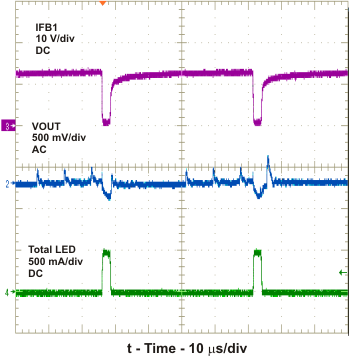
| Dimming waveform | 17 LEDs in series; VIN = 12 V; 22 kHz with 5% duty cycle | Figure 5 |
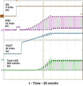
| Startup waveform | 17 LEDs in series; VIN = 12 V; 200 Hz with 50% duty cycle | Figure 6 |
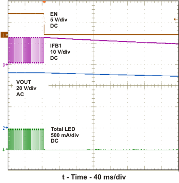
| Shutdown waveform | 17LEDs in series; VIN = 12 V; 200 Hz with 50% duty cycle | Figure 7 |
| Dimming efficiency | 17 LEDs in series; 200 Hz dimming frequency | Figure 9 |
| Dimming efficiency | 13 LEDs in series; 200 Hz dimming frequency | Figure 10 |
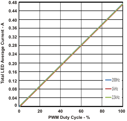 Figure 1. Dimming Linearity
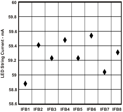 Figure 3. Current Matching
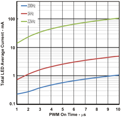 Figure 2. Dimming With Short On Time
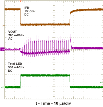 Figure 4. Dimming Waveforms
