SLVSAN3B December 2010 – November 2016 TPS61199
PRODUCTION DATA.
- 1 Features
- 2 Applications
- 3 Description
- 4 Revision History
- 5 Pin Configuration and Functions
- 6 Specifications
- 7 Detailed Description
- 8 Application and Implementation
- 9 Power Supply Recommendations
- 10Layout
- 11Device and Documentation Support
- 12Mechanical, Packaging, and Orderable Information
封装选项
机械数据 (封装 | 引脚)
散热焊盘机械数据 (封装 | 引脚)
- PWP|20
订购信息
10 Layout
10.1 Layout Consideration
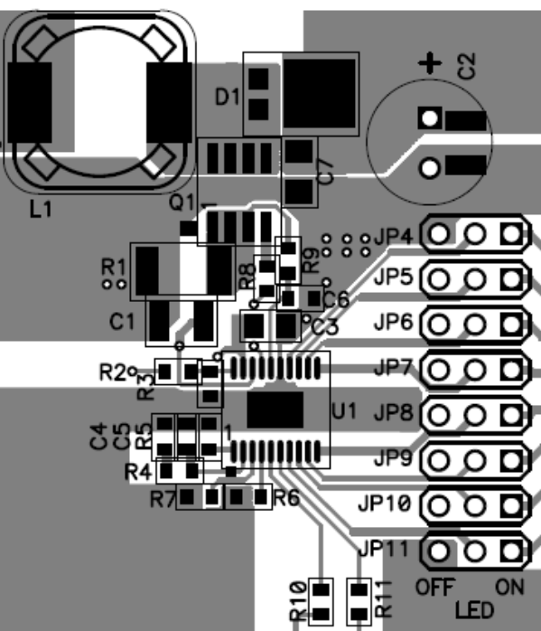
As for all switching power supplies, especially those providing high current and using high switching frequencies, layout is an important design step. If layout is not carefully done, the regulator could show instability as well as EMI problems. Therefore, use wide and short traces for high current paths. The VDD capacitor, C3 (see Typical Application) is the filter and noise decoupling capacitor for the internal linear regulator powering the internal digital circuits. Place C3 as close as possible between the VDD and GND pins to prevent any noise insertion to digital circuits. The switch node at the drain of Q1 carries high current with fast rising and falling edges. Therefore, the connection between this node to the inductor and the Schottky diode must be kept as short and wide as possible. It is also beneficial to have the ground of the output capacitor C2 close to the GND pin since there is large ground return current flowing between them. When laying out signal grounds, TI recommends using short traces separate from power ground traces, connecting them together at a single point, for example on the thermal pad in the PWP package. Resistors R5, R6, and R7 in Typical Application are LED short-protection threshold current setting and switching frequency programming resistors. To avoid unexpected noise coupling into the pins and affecting the accuracy, these resistors must be close to the pins with short and wide traces to GND. In the PWP package, the thermal pad must be soldered onto the PCB and connected to the GND pin of the device. Additional thermal via can significantly improve power dissipation of the device.
10.2 Layout Example
 Figure 14. Recommended TPS61199 PCB Layout