ZHCSEP0C October 2015 – February 2021 TPS61193
PRODUCTION DATA
- 1 特性
- 2 应用
- 3 说明
- 4 Revision History
- 5 Pin Configuration and Functions
-
6 Specifications
- 6.1 Absolute Maximum Ratings
- 6.2 ESD Ratings
- 6.3 Recommended Operating Conditions
- 6.4 Thermal Information
- 6.5 Electrical Characteristics (1) (1)
- 6.6 Internal LDO Electrical Characteristics
- 6.7 Protection Electrical Characteristics
- 6.8 Current Sinks Electrical Characteristics
- 6.9 PWM Brightness Control Electrical Characteristics
- 6.10 Boost and SEPIC Converter Characteristics
- 6.11 Logic Interface Characteristics
- 6.12 Typical Characteristics
- 7 Detailed Description
- 8 Application and Implementation
- 9 Power Supply Recommendations
- 10Layout
- 11Device and Documentation Support
- 12Mechanical, Packaging, and Orderable Information
7.3.1 Integrated DC-DC Converter
The TPS61193 DC-DC converter generates supply voltage for the LEDs and can operate in boost mode or in SEPIC mode. The maximum output voltage VOUT_MAX is defined by an external resistive divider (R1, R2).
VOUT_MAX voltage should be chosen based on the maximum voltage required for LED strings. Recommended maximum voltage is about 30% higher than maximum LED string voltage. DC-DC output voltage is adjusted automatically based on LED current sink headroom voltage. Maximum, minimum, and initial boost voltages can be calculated with Equation 1:
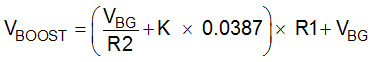
where
- VBG = 1.2 V
- R2 recommended value is 130 kΩ
- Resistor values are in kΩ
- K = 1 for maximum adaptive boost voltage (typical)
- K = 0 for minimum adaptive boost voltage (typical)
- K = 0.88 for initial boost voltage (typical)
 Figure 7-1 Maximum Converter Output Voltage vs R1 Resistance
Alternatively, a T-divider can be used if resistance less than 100 kΩ is required for the external resistive divider. Refer to Using the TPS61193EVM and TPS61193-Q1EVM Evaluation Module for details.
The converter is a current mode DC-DC converter, where the inductor current is measured and controlled with the feedback. Switching frequency is adjustable between 250 kHz and 2.2 MHz with RFSET resistor as Equation 2:
where
- ƒSW is switching frequency, kHz
- RFSET is frequency setting resistor, kΩ
In most cases lower frequency has higher system efficiency. DC-DC internal parameters are chosen automatically according to the selected switching frequency (see Table 7-2) to ensure stability. In boost mode a 15-pF capacitor CFB must be placed across resistor R1 when operating in 300-kHz to 500-kHz range (see Typical Application for 3 LED Strings). When operating in the 1.8-MHz to 2.2-MHz range CFB = 4.7 pF.
 Figure 7-2 Boost Block Diagram
DC-DC can be driven by an external SYNC signal between 300 kHz and 2.2 MHz. If the external synchronization input disappears, DC-DC continues operation at the frequency defined by RFSET resistor. When external frequency disappears and SYNC pin level is low, converter continues operation without spread spectrum immediately. If SYNC remains high, converter continues switching with spread spectrum enabled after 256 µs.
External SYNC frequency must be 1.2 to 1.5 times higher than the frequency defined by RFSET resistor. Minimum frequency setting with RFSET is 250 kHz to support 300-kHz switching with external clock.
The optional spread spectrum feature (±3% from central frequency, 1-kHz modulation frequency) reduces EMI noise at the switching frequency and its harmonic frequencies. When external synchronization is used, spread spectrum is not available.
| SYNC PIN INPUT | MODE |
|---|---|
| Low | Spread spectrum disabled |
| High | Spread spectrum enabled |
| 300 to 2200-kHz frequency | Spread spectrum disabled, external synchronization mode |
| RANGE | FREQUENCY (kHz) | TYPICAL INDUCTANCE (µH) | TYPICAL BOOST INPUT AND OUTPUT CAPACITORS (µF) | MINIMUM SWITCH OFF TIME (ns)(2) | BLANK TIME (ns) | CURRENT RAMP (A/s) | CURRENT RAMP DELAY (ns) |
|---|---|---|---|---|---|---|---|
| 1 | 300 to 480 | 33 | 2 ×10 (cer.) + 33 (electr.) | 150 | 95 | 24 | 550 |
| 2 | 480 to 1150 | 15 | 10 (cer.) + 33 (electr.) | 60 | 95 | 43 | 300 |
| 3 | 1150 to 1650 | 10 | 3 × 10 (cer.) | 40 | 95 | 79 | 0 |
| 4 | 1650 to 2200 | 4.7 | 3 × 10 (cer.) | 40 | 70 | 145 | 0 |
The converter SW pin DC current is limited to 2 A (typical). To support short-term transient conditions the current limit is automatically increased to 2.5 A for a short period of 1.5 seconds when a 2-A limit is reached.
Application condition where the 2-A limit is exceeded continuously is not allowed. In this case the current limit would be 2 A for 1.5 seconds followed by 2.5-A limit for 1.5 seconds, and this 3-second period repeats.
To keep switching voltage within safe levels there is a 48-V limit comparator in the event that FB loop is broken.