ZHCSG87E February 2017 – August 2019 TPS61178
PRODUCTION DATA.
- 1 特性
- 2 应用
- 3 说明
- 4 修订历史记录
- 5 Device Comparison Table
- 6 Pin Configuration and Functions
- 7 Specifications
-
8 Detailed Description
- 8.1 Overview
- 8.2 Functional Block Diagram
- 8.3
Feature Description
- 8.3.1 Under-voltage Lockout
- 8.3.2 Enable and Disable
- 8.3.3 Startup
- 8.3.4 Load Disconnect Gate Driver
- 8.3.5 Adjustable Peak Current Limit
- 8.3.6 Output Short Protection (with load disconnected FET)
- 8.3.7 Adjustable Switching Frequency
- 8.3.8 External Clock Synchronization (TPS611781)
- 8.3.9 Error Amplifier
- 8.3.10 Slope Compensation
- 8.3.11 Start-up with the Output Pre-Biased
- 8.3.12 Bootstrap Voltage (BST)
- 8.3.13 Over-voltage Protection
- 8.3.14 Thermal Shutdown
- 8.4 Device Functional Modes
-
9 Application and Implementation
- 9.1 Application Information
- 9.2
Typical Application
- 9.2.1 Design Requirements
- 9.2.2 Detailed Design Procedure
- 9.2.3 Setting the Current Limit
- 9.2.4 Setting the Output Voltage
- 9.2.5 TPS61178 Application Waveform
- 9.3 System Examples
- 10Power Supply Recommendations
- 11Layout
- 12器件和文档支持
- 13机械、封装和可订购信息
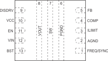
6 Pin Configuration and Functions
(RNW)
(13-Pin QFN)
Top View

Pin Functions
| PIN | I/O | DESCRIPTION | |
|---|---|---|---|
| NAME | NUMBER | ||
| FREQ / SYNC | 1 | I | The switching frequency is programmed by a resistor between this pin and the AGND. The internal oscillator can be synchronized by an external clock connecting into this pin. This pin can not be float in application. |
| AGND | 2 | - | Analog signal ground of the IC. Connect the AGND to PGND via a single point on the printed circuit board. |
| ILIMIT | 3 | I | Programming the switching peak current limit by a resistor between this pin and AGND. |
| COMP | 4 | O | Output of the internal error amplifier. The loop compensation network should be connected between this pin and AGND. |
| FB | 5 | I | Output voltage feedback, a resistor divider connecting to this pin sets the output voltage. |
| PGND | 6 | PWR | Power ground |
| SW | 7 | PWR | The switching node pin of the converter. It is connected to the drain of the internal low-side power FET and the source of the internal high-side power FET. |
| VOUT | 8 | PWR | Boost converter output |
| DISDRV | 9 | O | A gate drive output for the external disconnect FET. Connect the DISDRV pin to the gate of the external FET. Leave it floating if not using the load disconnect function. |
| VCC | 10 | O | Output of the internal regulator. A ceramic capacitor of more than 1.0 µF is required between this pin and ground |
| EN | 11 | I | Enable logic input. Logic high level enables the device and low level shutdown the device. |
| VIN | 12 | I | IC power supply input. |
| BST | 13 | O | Power supply for high-side FET gate driver. A capacitor must be connected between this pin and the SW pin |