ZHCSG87E February 2017 – August 2019 TPS61178
PRODUCTION DATA.
- 1 特性
- 2 应用
- 3 说明
- 4 修订历史记录
- 5 Device Comparison Table
- 6 Pin Configuration and Functions
- 7 Specifications
-
8 Detailed Description
- 8.1 Overview
- 8.2 Functional Block Diagram
- 8.3
Feature Description
- 8.3.1 Under-voltage Lockout
- 8.3.2 Enable and Disable
- 8.3.3 Startup
- 8.3.4 Load Disconnect Gate Driver
- 8.3.5 Adjustable Peak Current Limit
- 8.3.6 Output Short Protection (with load disconnected FET)
- 8.3.7 Adjustable Switching Frequency
- 8.3.8 External Clock Synchronization (TPS611781)
- 8.3.9 Error Amplifier
- 8.3.10 Slope Compensation
- 8.3.11 Start-up with the Output Pre-Biased
- 8.3.12 Bootstrap Voltage (BST)
- 8.3.13 Over-voltage Protection
- 8.3.14 Thermal Shutdown
- 8.4 Device Functional Modes
-
9 Application and Implementation
- 9.1 Application Information
- 9.2
Typical Application
- 9.2.1 Design Requirements
- 9.2.2 Detailed Design Procedure
- 9.2.3 Setting the Current Limit
- 9.2.4 Setting the Output Voltage
- 9.2.5 TPS61178 Application Waveform
- 9.3 System Examples
- 10Power Supply Recommendations
- 11Layout
- 12器件和文档支持
- 13机械、封装和可订购信息
9.2.4.4.3 Selecting the Disconnect FET
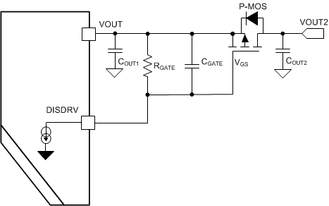
The TPS61178x provides a gate driver to control an external FET to disconnect the output from the input at shutdown or output short conditions, shown in Figure 25.
 Figure 25. Load Disconnect FET Connection
 The VDS, IDS and safe operation area (SOA) should be taken into consideration when selecting the FET:
- The drain-to-source voltage rating should be higher than the output max. voltage, VDS_DIS_MAX = VOUT,
- The drain-to-source RMS current rating is the maximum output current. I DS_DIS_RMS = IOUT,
- The SOA should be considered when the output short occurs, and there is heat caused by the short protection response time and surge current, SOA > QSHORT.
- VDS_DIS_Max is the maximum drain-source voltage
- IDS_DIS is the drain-source RMS current
- ISHORT is the short current
- TSHORT is the response time before the short protection triggered
- QSHORT is the heat produced for the output short

where
For instance: VOUT = 16 V, ISHORT = 20 A , TSHORT = 30 µs.
SOA ≥ 4.8 mJ, VDS_DIS_MAX ≥ 16 V.
The CSD25404Q3 –20 V P-Channel NexFET™ Power FET is used for this design example.
An additional capacitor between the gate and source of the external FET is required to slow the turn-on speed.

where
- TON_PFET is the on time of external FET
- VTH_PFET is the gate threshold of external FET
- CGS_PFET is the total gate capacitance of connected between gate and source external FET. (including the self-gate-source capacitance of the FET)
- IDIS_PFET is the discharge current inside of TPS61178x, it is 55 µA typically
Given 1.5 V threshold, CGS_PFET is 10 nF, the TON_PFET is around 300 µs.Please be aware that the maximum turn-on time should not exceed 3 ms, and the maximum capacitance CGS_PFET should be < 100 nF. Otherwise, the TPS61178x could not startup normally if the disconnect FET could not be turn on within the 3 ms.
The gate resistor depends on the gate-source voltage of the external FET,


Given the 5-V VGATE, the RGATE = 100 kΩ