SLVSBM5B December 2012 – August 2015 TPS61176
PRODUCTION DATA.
- 1 Features
- 2 Applications
- 3 Description
- 4 Revision History
- 5 Pin Configuration and Functions
- 6 Specifications
- 7 Detailed Description
- 8 Application and Implementation
- 9 Power Supply Recommendations
- 10Layout
- 11Device and Documentation Support
- 12Mechanical, Packaging, and Orderable Information
5 Pin Configuration and Functions
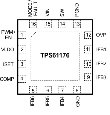
RTE Package
16-Pin WQFN with Exposed Thermal Pad
Top View

Pin Functions
| PIN | TYPE | DESCRIPTION | |
|---|---|---|---|
| NAME | NUMBER | ||
| COMP | 4 | Analog | Connect an external 0.47-µF ceramic capacitor to this pin for the boost loop compensation. |
| GND | 8 | Ground | Analog ground |
| IFB4 to IFB6, IFB1 to IFB3 |
5, 6, 7, 9, 10, 11 |
Analog | Regulated current sinks input pins |
| ISET | 3 | Analog | Full-scale LED current setting pin. Connect a resistor to the pin to program the full-scale LED current. |
| MODE/FAULT | 16 | Input | Multi-function pin. Use this pin to program the dimming mode. It also functions as a driver for external isolation P-channel MOSFET.(1) |
| OVP | 12 | Analog | This pin monitors the output voltage of the boost converter through external resistor divider. |
| PGND | 13 | Ground | Power ground |
| PWM/EN | 1 | Input | PWM dimming signal input and device enable / disable control.(1) |
| SW | 14 | Analog | Drain of the internal power MOSFET. |
| VIN | 15 | Power | Supply input pin, provides power supply to the device. |
| VLDO | 2 | Analog | Internal pre-regulator output. Connect a 1-µF ceramic capacitor to this pin. |
| Thermal Pad | — | — | The GND pin should be connected to the exposed thermal pad for proper operation. This thermal pad should be connected to any internal PCB ground plan using multiple vias for good thermal performance. |
(1) See Detailed Description for details.