SLVSBM5B December 2012 – August 2015 TPS61176
PRODUCTION DATA.
- 1 Features
- 2 Applications
- 3 Description
- 4 Revision History
- 5 Pin Configuration and Functions
- 6 Specifications
- 7 Detailed Description
- 8 Application and Implementation
- 9 Power Supply Recommendations
- 10Layout
- 11Device and Documentation Support
- 12Mechanical, Packaging, and Orderable Information
8 Application and Implementation
NOTE
Information in the following applications sections is not part of the TI component specification, and TI does not warrant its accuracy or completeness. TI’s customers are responsible for determining suitability of components for their purposes. Customers should validate and test their design implementation to confirm system functionality.
8.1 Application Information
The TPS61176 provides a high-performance LED lighting solution for tablets, notebooks and other low power LCD backlit displays. The device can drive 6 strings of 10 series LEDs in a compact and high efficient solution. The boost voltage can be set with a resistor divider on the OVP pin. The LED current is controlled via a logic level PWM input and the LED current level is set using an ISET resistor. Boost compensation can be adjusted using a capacitor on the COMP pin.
8.2 Typical Application
8.2.1 Single-Cell Battery Input Application
TPS61176's VIN pin voltage range is from 2.7 V to 6.5 V, so it can support single-cell battery input directly. If isolation MOSFET is connected, the mode resistor must be connected between VIN pin and MODE/FAULT pin as shown in Figure 9; if isolation MOSFET is not connected, the mode resistor can be connected between VIN pin and GND as shown in Figure 10. If there is no resistor connected at MODE/FAULT pin, which is only allowed when the isolation MOSFET is not connected, default mode (Mode 1) will be selected.
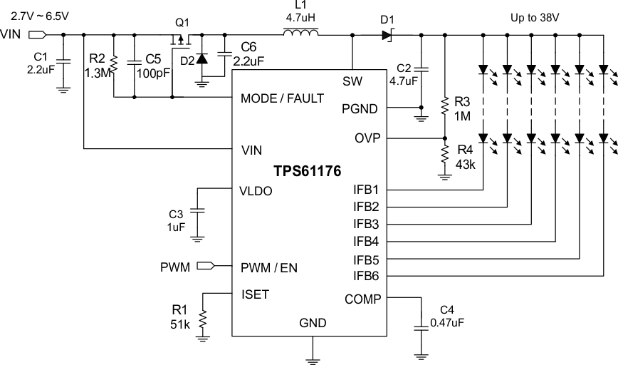 Figure 9. Typical Applications (Single-Cell Battery Input Application)
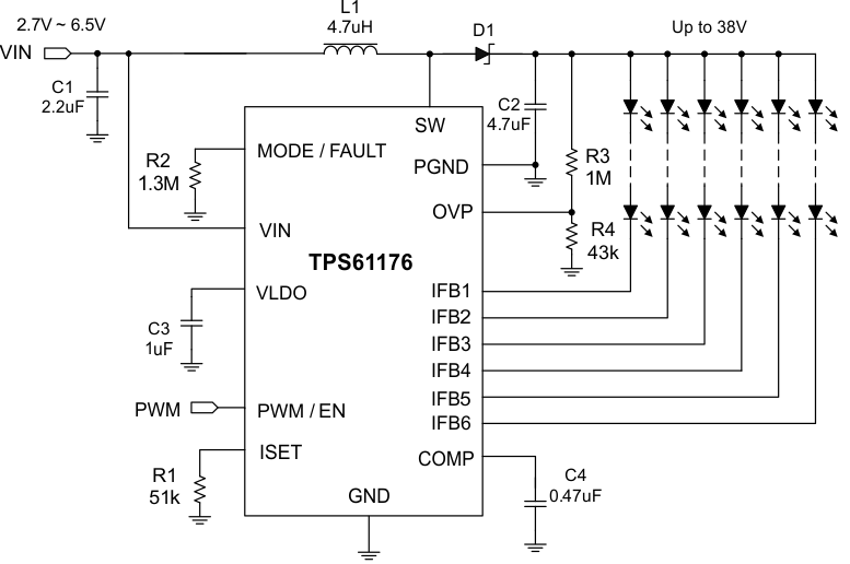 Figure 10. Typical Application (Single-Cell Battery Input Without Isolation MOSFET Application)
8.2.1.1 Design Requirements
For TPS61176 typical applications, use the parameters listed in Table 4 as input parameters.
Table 4. Design Parameters
| DESIGN PARAMETER | EXAMPLE VALUE |
|---|---|
| Minimum input voltage | 2.7 V |
| Output voltage | Up to 38 V |
| Number of series LED | up to 8 |
| Switching frequency | 1 MHz, typical |
| LED current | Up to 35 mA |
8.2.1.2 Detailed Design Procedure
8.2.1.2.1 Inductor Selection
Because the selection of the inductor affects the power supply steady-state operation, transient behavior, loop stability, and the boost converter efficiency, the inductor is the most important component in switching power regulator design. There are three specifications most important to the performance of the inductor: inductance value, DC resistance and saturation current. TPS61176 is designed to work with inductor values between 4.7 µH and 10 µH. A 4.7-µH inductor is typically available in a smaller or lower profile package, while a 10-µH inductor produces lower inductor ripple. If the boost output current is limited by the overcurrent protection of the device, using a 10-µH inductor can maximize the controller output current capability.
In a boost regulator, the inductor DC current can be calculated as Equation 5.

where
- Vout = boost output voltage
- Iout = boost output current
- Vin = boost input voltage
- η = power conversion efficiency, use 85% for TPS61176 normal applications
The inductor current peak-to-peak ripple can be calculated as Equation 6.

where
- IPP = inductor peak-to-peak ripple
- L = inductor value
- FS = Switching frequency
- Vout = boost output voltage
- Vin = boost input voltage
Therefore, the peak current seen by the inductor is calculated with Equation 7.

Select the inductor with saturation current over the calculated peak current. To calculate the worse case inductor peak current, use minimum input voltage, maximum output voltage and maximum load current.
Converter efficiency is dependent on the resistance of its high current path and switching losses associated with the internal switch and external power diode. Although the TPS61176 has optimized the internal switch resistance, the overall efficiency is affected by the inductor’s DC resistance (DCR). Lower DCR improves efficiency. However, there is a trade-off between DCR and inductor footprint. Furthermore, shielded inductors typically have higher DCR than unshielded ones.
Note that inductor values can have ±20% tolerance with no current bias. When the inductor current approaches saturation level, its inductance can decrease 20% to 35% from the 0-A value depending on how the inductor vendor defines saturation. Table 5 lists the recommended inductors.
Table 5. Recommended Inductors for the TPS61176
| PART NUMBER | L (µH) | DCR (mΩ) | ISAT (A) | SIZE (L x W x H mm) | VENDOR |
|---|---|---|---|---|---|
| PCMB051H-4R7MS | 4.7 | 78 | 4.0 | 5.4 x 5.2 x 1.8 | Cyntec |
| PCMB051H-6R8MS | 6.8 | 107 | 3.4 | 5.4 x 5.2 x 1.8 | Cyntec |
| PCMB051H-100MS | 10 | 140 | 3 | 5.4 x 5.2 x 1.8 | Cyntec |
| LPS4018-472ML | 4.7 | 125 | 1.9 | 4.0 x 4.0 x 1.8 | Coilcraft |
| LPS4018-103ML | 10 | 200 | 1.3 | 4.0 x 4.0 x 1.8 | Coilcraft |
| A915AY – 4R7M | 4.7 | 38 | 1.87 | 5.2 x 5.2 x 3 | TOKO |
| A915AY – 100M | 10 | 75 | 1.24 | 5.2 x 5.2 x 3 | TOKO |
8.2.1.2.2 Output Capacitor Selection
The output capacitor is mainly selected to meet the requirement for the loop stability and the output ripple. The loop is designed to be stable with an output capacitor within 2.2-µF to 10-µF range. This output ripple is related to the capacitor’s capacitance and its equivalent series resistance (ESR). Due to its low ESR, the ripple caused by ESR could be neglected for ceramic capacitors. Assuming a capacitor with zero ESR, the minimum capacitance needed for a given ripple can be calculated with Equation 8.

where
- Vripple = peak-to-peak output ripple.
Note that capacitor degradation increases the ripple much. Select the capacitor which has less degradation at the output voltage. If the output ripple is too large, change a bigger capacitor could be helpful. Normally, X5R ±10% or better capacitors are recommended.
8.2.1.2.3 Schottky Diode Selection
The TPS61176 demands a low forward voltage, high-speed rectification and low capacitance schottky diode for optimum efficiency. Ensure that the diode average and peak current rating exceeds the average output current and peak inductor current. In addition, the diode’s reverse breakdown voltage must exceed the open LED protection voltage. Vishay SS2P5, MSS1P4, and NXP PMEG4010EPK are recommended for the TPS61176.
8.2.1.2.4 Isolation FET Selection
The TPS61176 provides a gate driver at MODE/FAULT pin to drive an external P-channel MOSFET which can act as an isolation MOSFET. When the device is disabled or output short to ground issue happens, MODE/FAULT pin can turn off the isolation MOSFET to cut off the power path from the battery to the output. The source of the MOSFET should be connected to the battery input, and an external resistor must be connected between the source and gate of the MOSFET to keep the FET off when the device is disabled. This gate resistor also acts as a mode resistor to select the dimming mode. To turn on the isolation MOSFET, an internal current sink pulls MODE/FAULT pin low. When output short to ground fault happens, an internal switch pulls up the MODE/FAULT pin to VIN, turning off the isolation MOSFET immediately.
When the isolation FET is turned on during start-up, an inrush current will flow through the MOSFET from battery to charge the output capacitor. If the peak current is too large, a capacitor can be connected between the source and the gate of the isolation MOSFET to control the turning on speed (C5 in Figure 9), thus controlling the inrush current. Normally, a 100-pF to 1-nF capacitor is recommended.
During output short to ground protection process, the catch diode (D2 in Figure 9) may be forward biased to provide the continuous current of the inductor when the isolation FET is turned off. In this case, the drain of the isolation FET swings below ground. The voltage across the isolation FET can be momentarily greater than the input voltage. Therefore, select at least 10-V maximum input MOSFET. Adding a capacitor parallel with D2 (refer to Figure 9) could also help reduce the voltage across MOSFET when this failure happens. The ON resistance of the MOSFET has large impact on power conversion efficiency because the MOSFET carries the input current. Select a MOSFET with Rds(on) less than 100 mΩ to limit the power losses. In order to detect larger than 1 M RMode correctly, the gate leakage of isolation MOSFET should be less than 0.1 µA.
In multi-cell battery input applications, if the isolation MOSFET is connected, the voltage at MODE/FAULT pin may exceed its maximum rating voltage 7 V when the device is disabled or output short to ground issue happens. In order to prevent this over stress damange, isolation MOSFET can't be connected.
8.2.1.2.5 Audible Noise Reduction
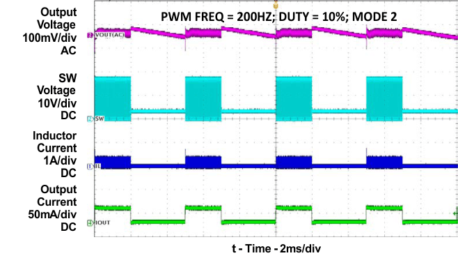
Output voltage of the controller also ripples due to the load transient that occurs during PWM dimming. If the PWM dimming frequency is in the audible frequency range, the ripple can produce audible noises on the output ceramic capacitor. There are two ways of reducing or eliminating the audible noise. The first way is to reduce the amount of the output ripple, and therefore minimize the audible noise. The TPS61176 adopts a patented technology to limit this type of output ripple even with the minimum recommended output capacitance. The second way is to select PWM dimming frequency outside the audible frequency range to eliminate the audible noise completely. However, in some applications, the input PWM signal frequency range couldn’t be adjusted outside the audible frequency range. To solve this problem, the device provides the 22-kHz fixed frequency PWM dimming mode. In this dimming mode, no matter what the input PWM frequency is, the PWM dimming is implemented at 22 kHz, which is outside the audible frequency range, saving the effort to adjust the input PWM frequency.
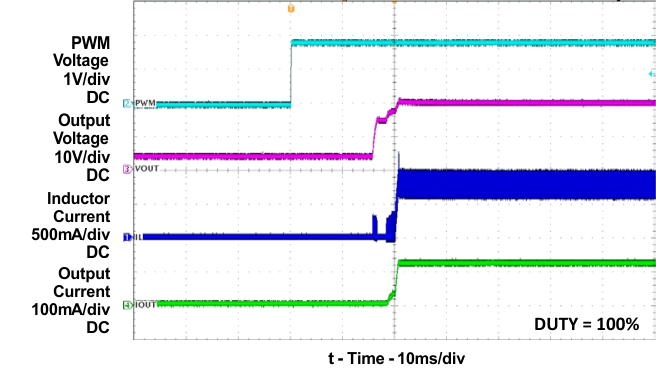
8.2.1.3 Application Curves
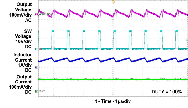
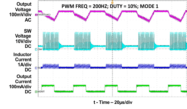
8.2.2 Multi-Cell Battery Input Application
In multi-cell battery input applications, because the normal input voltage is higher than the VIN pin and MODE/FAULT pin’s maximum rating voltage of 7 V, the battery input cannot be connected to VIN pin directly, nor can the isolation MOSFET. A 3.3-V or 5-V bias is required to power the VIN pin of the device with up to 3-mA current consumption, and the mode resistor should be connected between MODE/FAULT pin and ground. Refer to Figure 18.
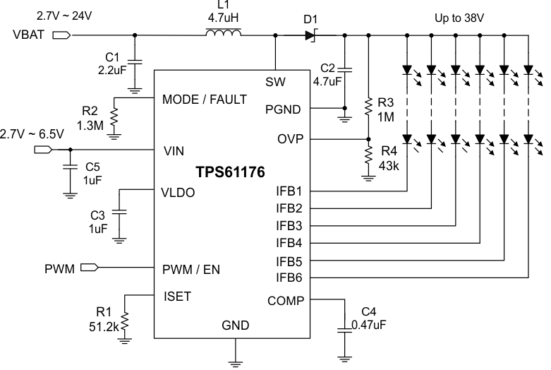 Figure 18. Typical Applications (Multi-Cell Battery Input Application)
8.2.3 Combined String Application
The TPS61176 provides six current sinks with up to 35-mA current capability each. If high brightness WLED diodes are used, the current sinks can be combined as two or three channels to support higher current capability requirement. Refer to Figure 19.
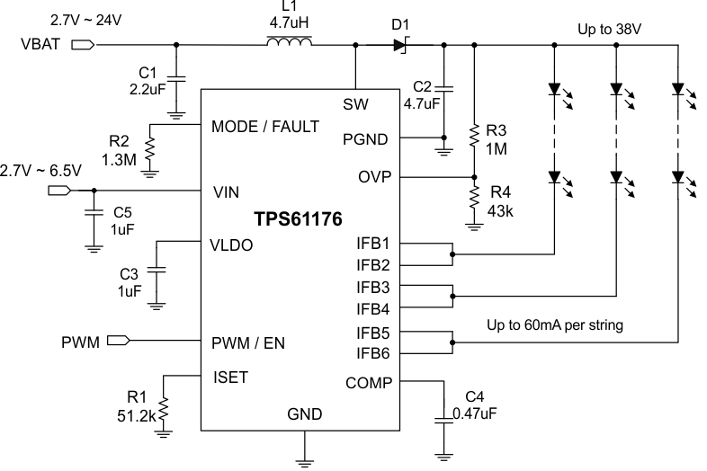 Figure 19. Typical Applications (Combined String to Support High Brightness WLED Diodes)
8.2.4 Separate PWM and EN Signals Application
The TPS61176 can be enabled or disabled automatically according to the PWM signal’s status. However, if the user wants to use separate EN and PWM signals to control the driver, the application circuit in Figure 20 or Figure 21 are recommended.
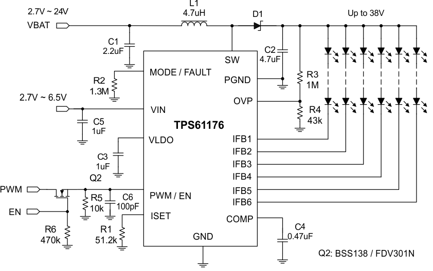 Figure 20. Typical Applications (to Support Separate 3.3-V Logic PWM and EN Signals)
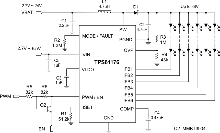 Figure 21. Typical Applications (to Support Separate 1.8-V Logic PWM and EN Signals)