ZHCSD56 December 2014 TPS61175-Q1
PRODUCTION DATA.
- 1 特性
- 2 应用范围
- 3 说明
- 4 简化电路原理图
- 5 修订历史记录
- 6 Pin Configuration and Functions
- 7 Specifications
- 8 Detailed Description
-
9 Application and Implementation
- 9.1 Application Information
- 9.2
Typical Application
- 9.2.1 Design Requirements
- 9.2.2
Detailed Design Procedure
- 9.2.2.1 Determining the Duty Cycle
- 9.2.2.2 Selecting the Inductor
- 9.2.2.3 Computing the Maximum Output Current
- 9.2.2.4 Setting Output Voltage
- 9.2.2.5 Setting the Switching Frequency
- 9.2.2.6 Setting the Soft Start Time
- 9.2.2.7 Selecting the Schottky Diode
- 9.2.2.8 Selecting the Input and Output Capacitors
- 9.2.2.9 Compensating the Small Signal Control Loop
- 9.2.3 Application Curves
- 10Power Supply Recommendations
- 11Layout
- 12器件和文档支持
- 13机械封装和可订购信息
6 Pin Configuration and Functions
TSSOP 14-PIN
(TOP VIEW)
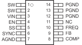
Pin Functions
| PIN | I/O | DESCRIPTION | |
|---|---|---|---|
| NAME | NO. | ||
| VIN | 3 | I | The input supply pin for the IC. Connect VIN to a supply voltage between 2.9 V and 18 V. It is acceptable for the voltage on the pin to be different from the boost power stage input for applications requiring voltage beyond VIN range. |
| SW | 1,2 | I | This is the switching node of the IC. Connect SW to the switched side of the indu1ctor. |
| FB | 9 | I | Feedback pin for positive voltage regulation. Connect to the center tap of a resistor divider to program the output voltage. |
| EN | 4 | I | Enable pin. When the voltage of this pin falls below the enable threshold for more than 10 ms, the IC turns off. |
| COMP | 8 | O | Output of the internal transconductance error amplifier. An external RC network is connected to this pin to compensate the regulator. |
| SS | 5 | O | Soft start programming pin. A capacitor between the SS pin and GND pin programs soft start timing. See application section for information on how to size the SS capacitor. |
| FREQ | 10 | O | Switch frequency program pin. An external resistor is connected to this pin to set switch frequency. See application section for information on how to size the FREQ resistor. |
| AGND | 7 | I | Signal ground of the IC |
| PGND | 12,13,14 | I | Power ground of the IC. It is connected to the source of the PWM switch. |
| SYNC | 6 | I | Switch frequency synchronous pin. Customers can use an external signal to set the IC switch frequency between 200-kHz and 2.2-MHz. If not used, this pin should be tied to AGND as short as possbile to avoid noise coupling. |
| NC | 11 | I | Reserved pin. Must connect this pin to ground. |
| Thermal Pad | The thermal pad should be soldered to the analog ground. If possible, use thermal via to connect to top and internal ground plane layers for ideal power dissipation. | ||