ZHCSD56 December 2014 TPS61175-Q1
PRODUCTION DATA.
- 1 特性
- 2 应用范围
- 3 说明
- 4 简化电路原理图
- 5 修订历史记录
- 6 Pin Configuration and Functions
- 7 Specifications
- 8 Detailed Description
-
9 Application and Implementation
- 9.1 Application Information
- 9.2
Typical Application
- 9.2.1 Design Requirements
- 9.2.2
Detailed Design Procedure
- 9.2.2.1 Determining the Duty Cycle
- 9.2.2.2 Selecting the Inductor
- 9.2.2.3 Computing the Maximum Output Current
- 9.2.2.4 Setting Output Voltage
- 9.2.2.5 Setting the Switching Frequency
- 9.2.2.6 Setting the Soft Start Time
- 9.2.2.7 Selecting the Schottky Diode
- 9.2.2.8 Selecting the Input and Output Capacitors
- 9.2.2.9 Compensating the Small Signal Control Loop
- 9.2.3 Application Curves
- 10Power Supply Recommendations
- 11Layout
- 12器件和文档支持
- 13机械封装和可订购信息
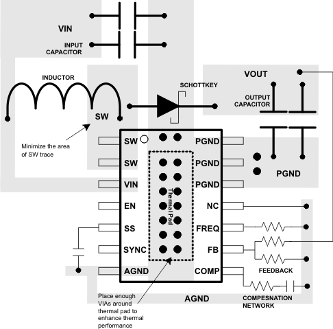
11 Layout
11.1 Layout Guidelines
- As for all switching power supplies, especially those running at high switching frequency and high currents, layout is an important design step. If layout is not carefully done, the regulator could suffer from instability as well as noise problems. To maximize efficiency, switch rise and fall times are fast. To prevent radiation of high frequency noise (this is, EMI), proper layout of the high frequency switching path is essential.
- Minimize the length and area of all traces connected to the SW pin and always use a ground plane under the switching regulator to minimize interplane coupling.
- The high current path including the switch, Schottky diode, and output capacitor, contains nanosecond rise and fall times and should be kept as short as possible.
- The input capacitor needs not only to be close to the VIN pin, but also to the GND pin in order to reduce the input supply ripple.
11.2 Layout Example
11.3 Thermal Considerations
The maximum IC junction temperature should be restricted to 125°C under normal operating conditions. This restriction limits the power dissipation of the TPS61175-Q1. Calculate the maximum allowable dissipation, PD(max), and keep the actual dissipation less than or equal to PD(max). The maximum-power-dissipation limit is determined using the following equation:
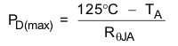
where, TA is the maximum ambient temperature for the application. RθJA is the thermal resistance junction-to-ambient given in the Thermal Information table.
The TPS61175-Q1 comes in a thermally enhanced TSSOP package. This package includes a thermal pad that improves the thermal capabilities of the package. The RθJA of the TSSOP package greatly depends on the PCB layout and thermal pad connection. The thermal pad must be soldered to the analog ground on the PCB. Using thermal vias underneath the thermal pad.