ZHCS629B December   2011  – May 2015 TPS61165-Q1

PRODUCTION DATA.  

  1. 特性
  2. 应用
  3. 说明
  4. 修订历史记录
  5. Pin Configuration and Functions
  6. Specifications
    1. 6.1 Absolute Maximum Ratings
    2. 6.2 ESD Ratings
    3. 6.3 Recommended Operating Conditions
    4. 6.4 Thermal Information
    5. 6.5 Electrical Characteristics
    6. 6.6 Timing Requirements
    7. 6.7 Typical Characteristics
  7. Detailed Description
    1. 7.1 Overview
    2. 7.2 Functional Block Diagram
    3. 7.3 Feature Description
      1. 7.3.1 Soft Start-Up
      2. 7.3.2 Open LED Protection
      3. 7.3.3 Undervoltage Lockout
      4. 7.3.4 Thermal Shutdown
    4. 7.4 Device Functional Modes
      1. 7.4.1 Shutdown
    5. 7.5 Programming
      1. 7.5.1 Current Program
      2. 7.5.2 LED Brightness Dimming Mode Selection
      3. 7.5.3 PWM Brightness Dimming
      4. 7.5.4 Digital 1 Wire Brightness Dimming
      5. 7.5.5 EasyScale: 1 Wire Digital Dimming
  8. Application and Implementation
    1. 8.1 Application Information
    2. 8.2 Typical Application
      1. 8.2.1 Design Requirements
      2. 8.2.2 Detailed Design Procedures
        1. 8.2.2.1 Maximum Output Current
        2. 8.2.2.2 Inductor Selection
        3. 8.2.2.3 Schottky Diode Selection
        4. 8.2.2.4 Compensation Capacitor Selection
        5. 8.2.2.5 Input and Output Capacitor Selection
      3. 8.2.3 Application Curves
    3. 8.3 Do's and Don'ts
  9. Power Supply Recommendations
  10. 10Layout
    1. 10.1 Layout Guidelines
    2. 10.2 Layout Example
    3. 10.3 Thermal Considerations
  11. 11器件和文档支持
    1. 11.1 器件支持
      1. 11.1.1 第三方产品免责声明
    2. 11.2 文档支持
      1. 11.2.1 相关文档 
    3. 11.3 社区资源
    4. 11.4 商标
    5. 11.5 静电放电警告
    6. 11.6 术语表
  12. 12机械、封装和可订购信息

封装选项

机械数据 (封装 | 引脚)
散热焊盘机械数据 (封装 | 引脚)
订购信息

Pin Configuration and Functions

DBV Package
6-Pin SOT-23
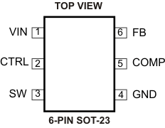
TPS61165-Q1 po_lvsb73.gif

Pin Functions

PIN I/O DESCRIPTION
NAME NO.
COMP 5 O Output of the transconductance error amplifier. Connect an external capacitor to this pin to compensate the converter.
CTRL 2 I Control pin of the boost converter. It is a multi-functional pin which can be used for enable control, PWM, and digital dimming.
FB 6 I Feedback pin for current. Connect the sense resistor from FB to GND.
GND 4 O Ground
SW 3 I This is the switching node of the IC. Connect the switched side of the inductor to SW. This pin is also used to sense the output voltage for open LED protection.
VIN 1 I The input supply pin for the IC. Connect VIN to a supply voltage between 3 V and 18 V.