ZHCSFM7C October   2016  – August 2023 TPS568215

PRODUCTION DATA  

  1.   1
  2. 特性
  3. 应用
  4. 说明
  5. Revision History
  6. Pin Configuration and Functions
  7. Specifications
    1. 6.1 Absolute Maximum Ratings
    2. 6.2 ESD Ratings
    3. 6.3 Recommended Operating Conditions
    4. 6.4 Thermal Information
    5. 6.5 Electrical Characteristics
    6. 6.6 Timing Requirements
    7. 6.7 Typical Characteristics
  8. Detailed Description
    1. 7.1 Overview
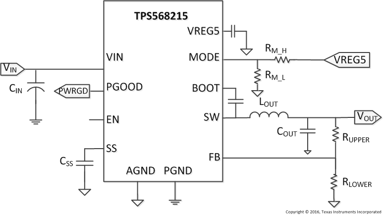
    2. 7.2 Functional Block Diagram
    3. 7.3 Feature Description
      1. 7.3.1  PWM Operation and D-CAP3 Control Mode
      2. 7.3.2  Eco-mode Control
      3. 7.3.3  4.7 V LDO and External Bias
      4. 7.3.4  MODE Selection
      5. 7.3.5  Soft Start and Pre-biased Soft Start
      6. 7.3.6  Enable and Adjustable UVLO
      7. 7.3.7  Power Good
      8. 7.3.8  Overcurrent Protection and Undervoltage Protection
      9. 7.3.9  Out-of-Bounds Operation
      10. 7.3.10 UVLO Protection
      11. 7.3.11 Thermal Shutdown
      12. 7.3.12 Output Voltage Discharge
    4. 7.4 Device Functional Modes
      1. 7.4.1 Light Load Operation
      2. 7.4.2 Standby Operation
  9. Application and Implementation
    1. 8.1 Application Information
    2. 8.2 Typical Application
      1. 8.2.1 Design Requirements
      2. 8.2.2 Detailed Design Procedure
        1. 8.2.2.1 External Component Selection
          1. 8.2.2.1.1 Output Voltage Set Point
          2. 8.2.2.1.2 Switching Frequency and Mode Selection
          3. 8.2.2.1.3 Inductor Selection
          4. 8.2.2.1.4 Output Capacitor Selection
          5. 8.2.2.1.5 Input Capacitor Selection
      3. 8.2.3 Application Curves
    3. 8.3 Power Supply Recommendations
    4. 8.4 Layout
      1. 8.4.1 Layout Guidelines
      2. 8.4.2 Layout Example
  10. Device and Documentation Support
    1. 9.1 Device Support
      1. 9.1.1 第三方产品免责声明
      2. 9.1.2 Development Support
    2. 9.2 接收文档更新通知
    3. 9.3 支持资源
    4. 9.4 Trademarks
    5. 9.5 静电放电警告
    6. 9.6 术语表
  11. 10Mechanical, Packaging, and Orderable Information

封装选项

机械数据 (封装 | 引脚)
散热焊盘机械数据 (封装 | 引脚)
订购信息

说明

TPS568215 是 TI 最小的一款单片 8A 同步降压转换器,具有自适应导通时间 D-CAP3™ 控制模式。该器件集成了 RDS(on) 较低的功率 MOSFET,简单易用并且高效运行,所需外部组件最少,适用于空间受限的电源系统。主要特性包括非常精确的基准电压、快速负载瞬态响应、自动跳跃模式运行以实现轻负载效率、可调节的电流限制和无需外部补偿。强制持续导通模式有助于满足高性能 DSP 和 FPGA 的严格电压调节精度要求。TPS568215 采用热增强型 18 引脚 HotRod QFN 封装,并且设计为在 -40°C 至 150°C 的结温范围内运行。TPS568215 与 TPS56C215 引脚兼容,因此用户可以在 6A 至 12A 范围内灵活选择采用同一封装的解决方案。

封装信息
器件型号封装(1)封装尺寸(标称值)
TPS568215RNN(VQFN,18)3.5mm x 3.5mm
如需了解所有可用封装,请参阅数据表末尾的可订购产品附录。
GUID-1F158D78-488B-4F8A-A69B-0A6FEC1A9C7B-low.gif
GUID-6BE23300-7F2D-4E44-A3CD-E7F6204A3F52-low.png