ZHCSI48B September   2017  – June 2018 TPS560430

UNLESS OTHERWISE NOTED, this document contains PRODUCTION DATA.  

  1. 特性
  2. 应用
  3. 说明
    1.     Device Images
      1.      简化原理图
      2.      效率与输出电流间的关系 VOUT = 5V,1100kHz,PFM
  4. 修订历史记录
  5. Device Comparison Table
  6. Pin Configuration and Functions
    1.     Pin Functions
  7. Specifications
    1. 7.1 Absolute Maximum Ratings
    2. 7.2 ESD Ratings
    3. 7.3 Recommended Operating Conditions
    4. 7.4 Thermal Information
    5. 7.5 Electrical Characteristics
    6. 7.6 Timing Requirements
    7. 7.7 Switching Characteristics
    8. 7.8 Typical Characteristics
  8. Detailed Description
    1. 8.1 Overview
    2. 8.2 Functional Block Diagram
    3. 8.3 Feature Description
      1. 8.3.1 Fixed Frequency Peak Current Mode Control
      2. 8.3.2 Adjustable Output Voltage
      3. 8.3.3 Enable
      4. 8.3.4 Minimum ON-Time, Minimum OFF-Time and Frequency Foldback
      5. 8.3.5 Bootstrap Voltage
      6. 8.3.6 Over Current and Short Circuit Protection
      7. 8.3.7 Soft Start
      8. 8.3.8 Thermal Shutdown
    4. 8.4 Device Functional Modes
      1. 8.4.1 Shutdown Mode
      2. 8.4.2 Active Mode
      3. 8.4.3 CCM Mode
      4. 8.4.4 Light-Load Operation (PFM Version)
      5. 8.4.5 Light-Load Operation (FPWM Version)
  9. Application and Implementation
    1. 9.1 Application Information
    2. 9.2 Typical Application
      1. 9.2.1 Design Requirements
      2. 9.2.2 Detailed Design Procedure
        1. 9.2.2.1 Custom Design With WEBENCH® Tools
        2. 9.2.2.2 Output Voltage Set-Point
        3. 9.2.2.3 Switching Frequency
        4. 9.2.2.4 Inductor Selection
        5. 9.2.2.5 Output Capacitor Selection
        6. 9.2.2.6 Input Capacitor Selection
        7. 9.2.2.7 Bootstrap Capacitor
        8. 9.2.2.8 Under Voltage Lockout Set-Point
      3. 9.2.3 Application Curves
  10. 10Power Supply Recommendations
  11. 11Layout
    1. 11.1 Layout Guidelines
      1. 11.1.1 Compact Layout for EMI Reduction
      2. 11.1.2 Feedback Resistors
    2. 11.2 Layout Example
  12. 12器件和文档支持
    1. 12.1 器件支持
      1. 12.1.1 开发支持
        1. 12.1.1.1 使用 WEBENCH® 工具创建定制设计
    2. 12.2 文档支持
      1. 12.2.1 相关文档
    3. 12.3 接收文档更新通知
    4. 12.4 社区资源
    5. 12.5 商标
    6. 12.6 静电放电警告
    7. 12.7 术语表
  13. 13机械、封装和可订购信息

封装选项

请参考 PDF 数据表获取器件具体的封装图。

机械数据 (封装 | 引脚)
  • DBV|6
散热焊盘机械数据 (封装 | 引脚)
订购信息

Adjustable Output Voltage

A precision 1.0-V reference voltage, VREF, is used to maintain a tightly regulated output voltage over the entire operating temperature range. The output voltage is set by a resistor divider from output voltage to the FB pin. It is recommended to use 1% tolerance resistors with a low temperature coefficient for the FB divider. Select the bottom-side resistor RFBB for the desired divider current and use Equation 1 to calculate top-side resistor RFBT. RFBT in the range from 10 kΩ to 100 kΩ is recommended for most applications. A lower RFBT value can be used if static loading is desired to reduce VOUT offset in PFM operation. Lower RFBT reduces efficiency at very light load. Less static current goes through a larger RFBT and might be more desirable when light-load efficiency is critical. But RFBT larger than 1 MΩ is not recommended because it makes the feedback path more susceptible to noise. Larger RFBT value requires more carefully designed feedback path on the PCB. The tolerance and temperature variation of the resistor dividers affect the output voltage regulation.
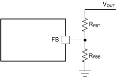
TPS560430 vout-set-slvse22.gifFigure 14. Output Voltage Setting
Equation 1. TPS560430 slvse22-equation-1.gif