ZHCS984B June 2012 – May 2019 TPS54678
PRODUCTION DATA.
- 1 特性
- 2 应用
- 3 说明
- 4 修订历史记录
- 5 Pin Configuration and Functions
- 6 Specifications
-
7 Detailed Description
- 7.1 Overview
- 7.2 Functional Block Diagram
- 7.3
Feature Description
- 7.3.1 Fixed Frequency PWM Control
- 7.3.2 Slope Compensation and Output Current
- 7.3.3 Bootstrap Voltage (Boot) and Low Dropout Operation
- 7.3.4 Error Amplifier
- 7.3.5 Voltage Reference
- 7.3.6 Adjusting the Output Voltage
- 7.3.7 Enable and Adjusting Undervoltage Lockout
- 7.3.8 Soft-Start Pin
- 7.3.9 Sequencing
- 7.3.10 Constant Switching Frequency and Timing Resistor (RT/CLK Pin)
- 7.3.11 Overcurrent Protection
- 7.3.12 Safe Start-Up into Prebiased Outputs
- 7.3.13 Synchronize Using the RT/CLK Pin
- 7.3.14 Power Good (PWRGD Pin)
- 7.3.15 Overvoltage Transient Protection
- 7.3.16 Thermal Shutdown
- 7.4 Device Functional Modes
-
8 Application and Implementation
- 8.1 Application Information
- 8.2
Typical Application
- 8.2.1 Design Requirements
- 8.2.2
Detailed Design Procedure
- 8.2.2.1 Custom Design With WEBENCH® Tools
- 8.2.2.2 Step One: Select the Switching Frequency
- 8.2.2.3 Step Two: Select the Output Inductor
- 8.2.2.4 Step Three: Choose the Output Capacitor
- 8.2.2.5 Step Four: Select the Input Capacitor
- 8.2.2.6 Step Five: Choose the Soft-Start Capacitor
- 8.2.2.7 Step Six: Select the Bootstrap Capacitor
- 8.2.2.8 Step Eight: Select Output Voltage and Feedback Resistors
- 8.2.2.9 Step Nine: Select Loop Compensation Components
- 8.2.3 Application Curves
- 9 Power Supply Recommendations
- 10Layout
- 11器件和文档支持
- 12机械、封装和可订购信息
7.4.1 Small Signal Model for Loop Response
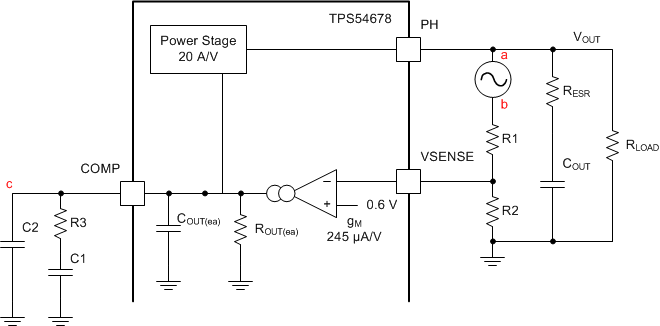
The Figure 26 shows an equivalent model for the TPS54678 control loop that can be modeled in a circuit simulation program to check frequency response and dynamic load response. The error amplifier is a transconductance amplifier with a gm of 245 µA/V. The error amplifier can be modeled using an ideal voltage controlled current source. The resistor RO and capacitor CO model the open loop gain and frequency response of the amplifier.
 Figure 26. Small Signal Model for Loop Response