ZHCSA92G August 2012 – June 2018 TPS54360
PRODUCTION DATA.
- 1 特性
- 2 应用
- 3 说明
- 4 修订历史记录
- 5 Pin Configuration and Functions
- 6 Specifications
-
7 Detailed Description
- 7.1 Overview
- 7.2 Functional Block Diagram
- 7.3
Feature Description
- 7.3.1 Fixed Frequency PWM Control
- 7.3.2 Slope Compensation Output Current
- 7.3.3 Pulse Skip Eco-mode
- 7.3.4 Low Dropout Operation and Bootstrap Voltage (BOOT)
- 7.3.5 Error Amplifier
- 7.3.6 Adjusting the Output Voltage
- 7.3.7 Enable and Adjusting Undervoltage Lockout
- 7.3.8 Internal Soft-Start
- 7.3.9 Constant Switching Frequency and Timing Resistor (RT/CLK) Terminal)
- 7.3.10 Accurate Current Limit Operation and Maximum Switching Frequency
- 7.3.11 Synchronization to RT/CLK Terminal
- 7.3.12 Overvoltage Protection
- 7.3.13 Thermal Shutdown
- 7.3.14 Small Signal Model for Loop Response
- 7.3.15 Simple Small Signal Model for Peak Current Mode Control
- 7.3.16 Small Signal Model for Frequency Compensation
- 7.4 Device Functional Modes
-
8 Application and Implementation
- 8.1 Application Information
- 8.2
Typical Application
- 8.2.1 Design Requirements
- 8.2.2
Detailed Design Procedure
- 8.2.2.1 Custom Design with WEBENCH® Tools
- 8.2.2.2 Selecting the Switching Frequency
- 8.2.2.3 Output Inductor Selection (LO)
- 8.2.2.4 Output Capacitor
- 8.2.2.5 Catch Diode
- 8.2.2.6 Input Capacitor
- 8.2.2.7 Bootstrap Capacitor Selection
- 8.2.2.8 Undervoltage Lockout Set Point
- 8.2.2.9 Output Voltage and Feedback Resistors Selection
- 8.2.2.10 Minimum VIN
- 8.2.2.11 Compensation
- 8.2.2.12 Discontinuous Conduction Mode and Eco-mode Boundary
- 8.2.2.13 Power Dissipation Estimate
- 8.2.3 Application Curves
- 9 Power Supply Recommendations
- 10Layout
- 11器件和文档支持
- 12机械、封装和可订购信息
7.3.14 Small Signal Model for Loop Response
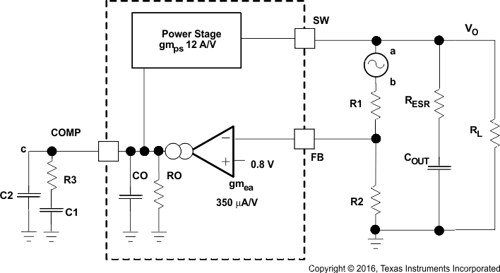
Figure 28 shows an equivalent model for the TPS54360 control loop which can be simulated to check the frequency response and dynamic load response. The error amplifier is a transconductance amplifier with a gmEA of 350 μA/V. The error amplifier can be modeled using an ideal voltage controlled current source. The resistor Ro and capacitor Co model the open loop gain and frequency response of the amplifier. The 1mV ac voltage source between the nodes a and b effectively breaks the control loop for the frequency response measurements. Plotting c/a provides the small signal response of the frequency compensation. Plotting a/b provides the small signal response of the overall loop. The dynamic loop response can be evaluated by replacing RL with a current source with the appropriate load step amplitude and step rate in a time domain analysis. This equivalent model is only valid for continuous conduction mode (CCM) operation.
 Figure 28. Small Signal Model for Loop Response