ZHCSFM8A December   2011  – October 2016 TPS53313

PRODUCTION DATA.  

  1. 特性
  2. 应用
  3. 说明
  4. 修订历史记录
  5. Pin Configuration and Functions
  6. Specifications
    1. 6.1 Absolute Maximum Ratings
    2. 6.2 ESD Ratings
    3. 6.3 Recommended Operating Conditions
    4. 6.4 Thermal Information
    5. 6.5 Electrical Characteristics
    6. 6.6 Typical Characteristics
  7. Detailed Description
    1. 7.1 Overview
    2. 7.2 Functional Block Diagram
    3. 7.3 Feature Description
      1. 7.3.1 Soft-Start Operation
      2. 7.3.2 Power Good
      3. 7.3.3 UVLO Function
      4. 7.3.4 Overcurrent (OC) Protection
      5. 7.3.5 Overvoltage and Undervoltage Protection
      6. 7.3.6 Overtemperature Protection
      7. 7.3.7 Output Discharge
      8. 7.3.8 Switching Frequency Setting and Synchronization
    4. 7.4 Device Functional Modes
      1. 7.4.1 Operation Mode
      2. 7.4.2 Light Load Operation
      3. 7.4.3 Forced Continuous Conduction Mode
  8. Application and Implementation
    1. 8.1 Application Information
    2. 8.2 Typical Application
      1. 8.2.1 Design Requirements
      2. 8.2.2 Detailed Design Procedure
        1. 8.2.2.1 Output Inductor Selection
        2. 8.2.2.2 Output Capacitor Selection
        3. 8.2.2.3 Input Capacitor Selection
        4. 8.2.2.4 Output Voltage Setting Resistors Selection
        5. 8.2.2.5 Compensation Design
      3. 8.2.3 Application Curves
  9. Power Supply Recommendations
  10. 10Layout
    1. 10.1 Layout Guidelines
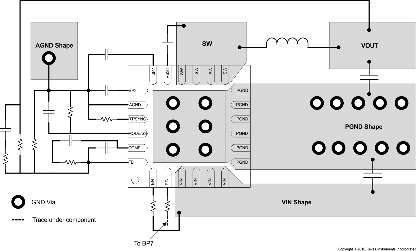
    2. 10.2 Layout Example
  11. 11器件和文档支持
    1. 11.1 接收文档更新通知
    2. 11.2 社区资源
    3. 11.3 商标
    4. 11.4 静电放电警告
    5. 11.5 Glossary
  12. 12机械、封装和可订购信息

封装选项

机械数据 (封装 | 引脚)
散热焊盘机械数据 (封装 | 引脚)
订购信息

Layout

Layout Guidelines

Good layout is essential for stable power supply operation. Follow these guidelines for an efficient PCB layout:

  • Separate the power ground and analog ground planes. Connect them together at one location.
  • Use 6 vias to connect the thermal pad to power ground.
  • Place VIN, BP7 and BP3 decoupling capacitors as close to the device as possible.
  • Use wide traces for VIN, PGND and SW. These nodes carry high-current and also serve as heat sinks.
  • Place feedback and compensation components as close to the device as possible.
  • Keep analog signals (FB, COMP) away from noisy signals (SW, VBST).

Layout Example

TPS53313 TPS53313Layout.gif Figure 26. TPS53313 Layout Example