ZHCSDD2A January 2015 – February 2015 TPS24740 , TPS24741 , TPS24742
PRODUCTION DATA.
- 1 特性
- 2 应用
- 3 说明
- 4 简化电路原理图
- 5 修订历史记录
- 6 Device Comparison Table
- 7 Pin Configuration and Functions
- 8 Specifications
-
9 Detailed Description
- 9.1 Overview
- 9.2 Functional Block Diagram
- 9.3
Feature Description
- 9.3.1 Internal Power ORing of TPS24740
- 9.3.2 Enable and Over-voltage Protection
- 9.3.3 Current Limit and Power Limit During Start-up
- 9.3.4 Two Level Protection During Regular Operation
- 9.3.5 Dual Timer (TFLT and TINR)
- 9.3.6 Using SoftStart - IHGATE and TINR Considerations
- 9.3.7 Three Options for Response to a Fast Trip
- 9.3.8 Programmable Reverse Voltage Threshold
- 9.3.9 Analog Current Monitor
- 9.3.10 Power Good Flag
- 9.3.11 ORing MOSFET Status Indicator
- 9.3.12 Fault Reporting
- 9.4 Device Functional Modes
-
10Application and Implementation
- 10.1 Application Information
- 10.2
Typical Application
- 10.2.1 30A Single channel OR then Hot Swap With Current Monitoring
- 10.2.2 Design Requirements
- 10.2.3
Detailed Design Procedure
- 10.2.3.1 Select RSNS and VSNS,CL Setting
- 10.2.3.2 Selecting the Fast Trip Threshold and Filtering
- 10.2.3.3 Selecting the Hot Swap FET(s)
- 10.2.3.4 Select Power Limit
- 10.2.3.5 Set Fault Timer
- 10.2.3.6 Check MOSFET SOA
- 10.2.3.7 Choose ORing MOSFET
- 10.2.3.8 Choose Reverse Current Threshold and Filtering
- 10.2.3.9 Choose Under Voltage and Over Voltage Settings
- 10.2.3.10 Selecting CIN, COUT, and CMIDDLE
- 10.2.3.11 Selecting D1 and D2
- 10.2.3.12 Ensuring Stability
- 10.2.3.13 Compute Tolerances
- 10.2.4 Application Curves
- 10.2.5
40 A Single Channel Hot Swap then ORing
- 10.2.5.1 Design Requirements
- 10.2.5.2
Design Procedure
- 10.2.5.2.1 Select RSNS and VSNS,CL Setting
- 10.2.5.2.2 Selecting the Fast Trip Threshold and Filtering
- 10.2.5.2.3 Selecting the Hot Swap FET
- 10.2.5.2.4 Select Power Limit
- 10.2.5.2.5 Set Fault Timer
- 10.2.5.2.6 Check MOSFET SOA
- 10.2.5.2.7 Checking Stability of Hot Swap Loop
- 10.2.5.2.8 Choose ORing MOSFET
- 10.2.5.2.9 Choose Reverse Current Threshold and Filtering
- 10.2.5.2.10 Choose Under Voltage and Over Voltage Settings
- 10.2.5.2.11 Selecting CIN, COUT, CMIDDLE, and Transient Protection
- 10.2.5.2.12 Adding CENHS
- 10.2.5.3 Application Curves
- 10.3 System Examples
- 11Power Supply Recommendations
- 12Layout
- 13器件和文档支持
- 14机械封装和可订购信息
封装选项
机械数据 (封装 | 引脚)
- RGE|24
散热焊盘机械数据 (封装 | 引脚)
- RGE|24
订购信息
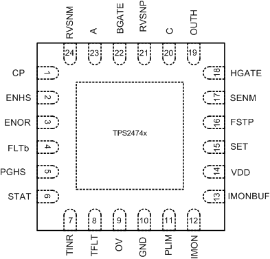
7 Pin Configuration and Functions
QFN 24-Pin with Thermal Pad
RGE Package
Top View

Table 1. Pin Functions
| PIN | TYPE(1) | DESCRIPTION | |
|---|---|---|---|
| NAME | NO. | ||
| A | 23 | I/P | Voltage sense input that connects to the OR MOSFET's body diode's anode. Connect to the OR MOSFET source in the typical configuration. A pin is used to supply power to the ORing block of the TPS2474x under certain biasing conditions. |
| BGATE | 22 | O | Connect to the gate of the external OR MOSFET. Controls the OR MOSFET to emulate a low forward-voltage diode. |
| C | 20 | I/P | Voltage sense input that connects to the OR MOSFET's body diode's cathode. Connect to the OR MOSFET drain in the typical configuration. C pin is used to supply power to the ORing block of the TPS2474x under certain biasing conditions. |
| CP | 1 | I/O | Connect a storage capacitor from CP to A for fast turn-on of blocking Gate. |
| ENHS | 2 | I | Active-high enable input of Hot-swap. Logic input. Connects to resistor divider. |
| ENOR | 3 | I | Active-high enable input of Oring. Logic input. Connects to resistor divider. |
| FLTb | 4 | O | Active-low, open-drain output indicating various faults. |
| FSTP | 16 | I | Fast trip programming set pin for hot-swap. A resistor is connected from positive terminal of the sensing resistor to FSTP. |
| GND | 10 | – | Ground. |
| HGATE | 18 | O | Gate driver output for external Hot Swap MOSFET. |
| IMON | 12 | I/O | Analog current monitor and load current limit program point. Connect RIMON to ground. |
| IMONBUF | 13 | O | Voltage output proportional to the load current (0V–3.0V). |
| OUTH | 19 | I | Output voltage sensor for monitoring Hot Swap MOSFET power. Connects to the source terminal of the hot-swap N channel MOSFET. |
| OV | 9 | I | Overvoltage comparator input. Connects to resistor divider. HGATE and BGATE are pulled low when OV exceeds the threshold. Connect to ground when not used. |
| PGHS | 5 | O | Active-high, open-drain power-good indicator. |
| PLIM | 11 | I | Power-limiting programming pin. A resistor from this pin to GND sets the maximum power dissipation for the Hot Swap FET. |
| RVSNP | 21 | I | Positive input of the reverse voltage comparator. Connect a resistor from RVSNP to C to set the reverse voltage trip point of the blocking FET. |
| RVSNM | 24 | I | Negative input of the reverse voltage comparator. |
| SENM | 17 | I | Current-sensing input for the sensing resistor. Directly connects to the negative terminal of the sensing resistor. |
| SET | 15 | I | Current-limit programming set pin for hot-swap. A resistor is connected from positive terminal of the sensing resistor. |
| STAT | 6 | O | High when BGATE is ON. |
| TFLT | 8 | I/O | Fault timer, which runs when the device goes from regular operation to an over-current condition. |
| TINR | 7 | I/O | Inrush timer, which runs during the inrush operation (start-up) if the part is in current limit or power limit. |
| VDD | 14 | P | Power Supply. |
(1) I = Input; O = Output ; P = Power