ZHCS845A March 2012 – July 2015 TPS2379
PRODUCTION DATA.
- 1 特性
- 2 应用
- 3 说明
- 4 修订历史记录
- 5 Pin Configuration and Functions
- 6 Specifications
- 7 Parameter Measurement Information
-
8 Detailed Description
- 8.1 Overview
- 8.2 Functional Block Diagram
- 8.3 Feature Description
- 8.4
Device Functional Modes
- 8.4.1
PoE Overview
- 8.4.1.1 Threshold Voltages
- 8.4.1.2 PoE Start-Up Sequence
- 8.4.1.3 Detection
- 8.4.1.4 Hardware Classification
- 8.4.1.5 Inrush and Start-up
- 8.4.1.6 Maintain Power Signature
- 8.4.1.7 Start-up and Operation
- 8.4.1.8 PD Hotswap Operation
- 8.4.1.9 CDB and T2P
- 8.4.1.10 Auxiliary Pass MOSFET Control
- 8.4.1.11 Using DEN to Disable PoE
- 8.4.1
PoE Overview
- 9 Application and Implementation
- 10Power Supply Recommendations
- 11Layout
- 12器件和文档支持
- 13机械、封装和可订购信息
6 Specifications
6.1 Absolute Maximum Ratings
over operating free-air temperature range (unless otherwise noted) (1)| MIN | MAX | UNIT | ||
|---|---|---|---|---|
| Input voltage | VDD, DEN | –0.3 | 100 | V |
| RTN(2) | –0.6 | 100 | ||
| CLS(3) | –0.3 | 6.5 | ||
| GATE(3) | –0.3 | 18 | ||
| [CDB, T2P] to RTN | –0.3 | 100 | ||
| Sinking current | RTN(4) | Internally limited | mA | |
| CDB, T2P | 5 | |||
| DEN | 1 | |||
| Sourcing current | CLS | 65 | mA | |
| TJMAX | Internally limited | °C | ||
| Storage temperature, Tstg | –65 | 150 | °C | |
(1) Stresses beyond those listed under Absolute Maximum Ratings may cause permanent damage to the device. These are stress ratings only, which do not imply functional operation of the device at these or any other conditions beyond those indicated under Recommended Operating Conditions. Exposure to absolute-maximum-rated conditions for extended periods may affect device reliability.
(2) With I(RTN) = 0
(3) Do not apply voltages to these pins
(4) SOA limited to RTN = 80 V at 1.2 A.
6.2 ESD Ratings
| VALUE | UNIT | ||||
|---|---|---|---|---|---|
| V(ESD) | Electrostatic discharge | Human body model (HBM), per ANSI/ESDA/JEDEC JS-001, all pins(1) | 2000 | V | |
| Charged device model (CDM), per JEDEC specification JESD22-C101, all pins(2) | 500 | ||||
| IEC 61000-4-2 contact discharge(3) | 8000 | ||||
| IEC 61000-4-2 air-gap discharge(3) | 15000 | ||||
(1) JEDEC document JEP155 states that 500-V HBM allows safe manufacturing with a standard ESD control process.
(2) JEDEC document JEP157 states that 250-V CDM allows safe manufacturing with a standard ESD control process.
(3) Discharges applied to circuit of Figure 26 between RJ-45, adapter, and output voltage rails.
6.3 Recommended Operating Conditions
Voltages with respect to VSS (unless otherwise noted)| MIN | NOM | MAX | UNIT | ||
|---|---|---|---|---|---|
| Input voltage range | RTN, VDD | 0 | 57 | V | |
| T2P or CDB to RTN | 0 | 57 | |||
| Sinking current | RTN | 0.85 | A | ||
| CDB, T2P | 2 | mA | |||
| Resistance | CLS(1) | 60 | Ω | ||
| Junction temperature | –40 | 125 | °C | ||
(1) Voltage should not be externally applied to this pin.
6.4 Thermal Information
| THERMAL METRIC(1) | TPS2379 | UNIT | |
|---|---|---|---|
| DDA (HSOP) | |||
| 8 PINS | |||
| RθJA | Junction-to-ambient thermal resistance | 45.9 | °C/W |
| RθJC(top) | Junction-to-case (top) thermal resistance | 51.9 | °C/W |
| RθJB | Junction-to-board thermal resistance | 28.8 | °C/W |
| ψJT | Junction-to-top characterization parameter | 8.9 | °C/W |
| ψJB | Junction-to-board characterization parameter | 28.7 | °C/W |
| RθJC(bot) | Junction-to-case (bottom) thermal resistance | 6.7 | °C/W |
(1) For more information about traditional and new thermal metrics, see the Semiconductor and IC Package Thermal Metrics application report, SPRA953.
6.5 Electrical Characteristics
40 V ≤ VVDD ≤ 57 V, RDEN = 24.9 kΩ, CDB, CLS, GATE, T2P open; –40°C ≤ TJ ≤ 125°C. Positive currents are into pins. Typical values are at 25°C. All voltages are with respect to VVSS (unless otherwise noted)| PARAMETER | TEST CONDITIONS | MIN | TYP | MAX | UNIT | |
|---|---|---|---|---|---|---|
| DETECTION (DEN) | ||||||
| Detection current | Measure ISUPPLY(VDD, RTN, DEN) | µA | ||||
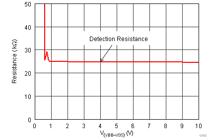
| VDD = 1.4 V | 53.8 | 56.5 | 58.3 | |||
| VDD = 10.1 V, Not in mark | 395 | 410 | 417 | |||
| Bias current | DEN open, VVDD = 10.1 V, Measure ISUPPLY, Not in mark | 3 | 4.8 | 12 | µA | |
| VPD_DIS | Disable threshold | DEN falling | 3 | 3.7 | 5 | V |
| Hysteresis | 50 | 113 | 200 | mV | ||
| CLASSIFICATION (CLS) | ||||||
| ICLS | Classification current | 13 V ≤ VDD ≤ 21 V, Measure IVDD + IDEN + IRTN | ||||
| RCLS = 1270 Ω | 1.8 | 2.17 | 2.6 | mA | ||
| RCLS = 243 Ω | 9.9 | 10.6 | 11.2 | |||
| RCLS = 137 Ω | 17.6 | 18.6 | 19.4 | |||
| RCLS = 90.9 Ω | 26.5 | 27.9 | 29.3 | |||
| RCLS = 63.4 Ω | 38 | 39.9 | 42 | |||
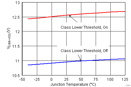
| VCL_ON | Class lower threshold | VDD rising, VCLS ↑ | 11.9 | 12.5 | 13 | V |
| Hysteresis | 1.4 | 1.6 | 1.7 | |||
| VCL_H | ||||||
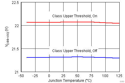
| VCU_ON | Class upper threshold | VDD rising, VCLS↓ | 21 | 22 | 23 | V |
| VCU_H | Hysteresis | 0.5 | 0.78 | 0.9 | ||
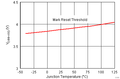
| VMSR | Mark reset threshold | VVDD falling | 3 | 3.9 | 5 | |
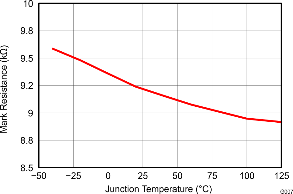
| Mark state resistance | 2-point measurement at 5 V and 10.1 V | 6 | 10 | 12 | kΩ | |
| Leakage current | VDD = 57 V, VCLS = 0 V, measure ICLS | 1 | µA | |||
| GATE (AUXILIARY GATE OUTPUT) | ||||||
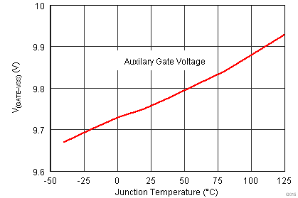
| Output high voltage | 8 | 10 | 12 | V | ||
| Sourcing current | VGATE = 0 V | 25 | 38 | 60 | µA | |
| Sinking current | VGATE = 4 V, VDD = 48→ 25 V | 0.6 | 1.25 | 1.75 | mA | |
| VDD = 25 V, VGATE = 0→ 4 V | 5 | 23.2 | 30 | |||
| Current limit delay | 150 | 365 | 600 | µs | ||
| PASS DEVICE (RTN) | ||||||
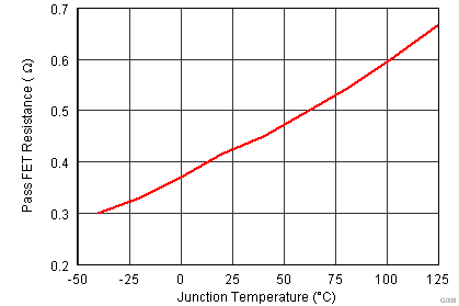
| rDS(ON) | On resistance | 0.2 | 0.42 | 0.75 | Ω | |
| Input bias current | VDD = VRTN = 30 V, measure IRTN | 30 | µA | |||
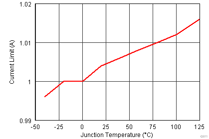
| Current limit | VRTN =1.5 V | 0.85 | 1 | 1.2 | A | |
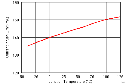
| Inrush current limit | VRTN = 2 V, VDD: 20 V → 48 V | 100 | 140 | 180 | mA | |
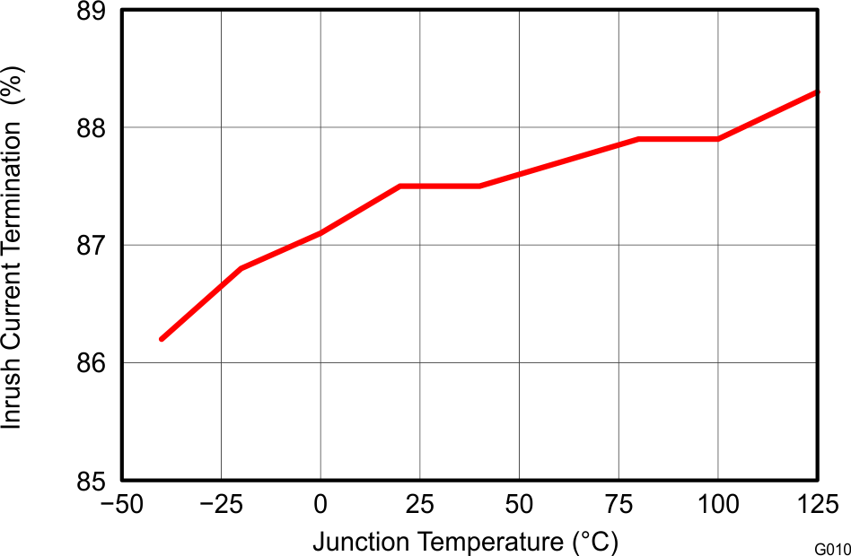
| Inrush termination | Percentage of inrush current | 80% | 90% | 99% | ||
| Foldback threshold | VRTN rising | 11 | 12.3 | 13.6 | V | |
| Foldback deglitch time | VRTN rising to when current limit changes to inrush current limit | 500 | 800 | 1500 | µs | |
| CONVERTER DISABLE (CDB) | ||||||
| Output low voltage | ICDB = 2 mA, VRTN = 2 V, VDD: 20 V → 48 V | 0.27 | 0.50 | V | ||
| Minimum voltage, V(VDD –RTN), for CDB to be valid | VCDB = VDD, ICDB = 1 mA, in inrush | 3 | V | |||
| Leakage current | VCDB = 57 V, VRTN = 0 V | 10 | µA | |||
| TYPE 2 PSE INDICATION (T2P) | ||||||
| VT2P | Output low voltage | IT2P = 2 mA, after 2-event classification and inrush is complete, VRTN = 0 V | 0.26 | 0.60 | V | |
| Leakage current | VT2P = 57 V, VRTN = 0 V | 10 | µA | |||
| UVLO | ||||||
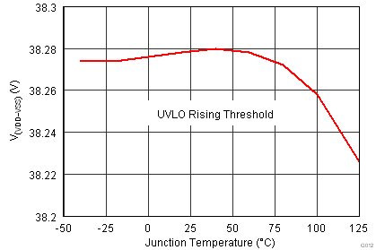
| VUVLO_R | UVLO rising threshold | VVDD rising | 36.3 | 38.1 | 40 | V |
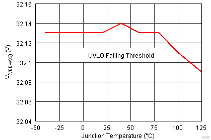
| UVLO falling threshold | VVDD falling | 30.5 | 32 | 33.6 | ||
| VUVLO_H | UVLO hysteresis | 6.1 | V | |||
| THERMAL SHUTDOWN | ||||||
| Shutdown | TJ↑ | 135 | 145 | °C | ||
| Hysteresis | 20 | |||||
| VDD BIAS CURRENT | ||||||
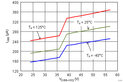
| Operating current | 40 V ≤ VVDD ≤ 57 V | 285 | 500 | µA | ||
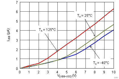
6.6 Typical Characteristics
