ZHCSHW4A December 2017 – January 2019 TPS23523
PRODUCTION DATA.
- 1 特性
- 2 应用
- 3 说明
- 4 修订历史记录
- 5 Pin Configuration and Functions
- 6 Specifications
- 7 Parameter Measurement Information
- 8 Detailed Description
-
9 Application and Implementation
- 9.1 Application Information
- 9.2
Typical Application
- 9.2.1 Design Requirements
- 9.2.2
Detailed Design Procedure
- 9.2.2.1 Selecting RSNS
- 9.2.2.2 Selecting Soft Start Setting: CSS and CSS,VEE
- 9.2.2.3 Selecting VDS Switch Over Threshold
- 9.2.2.4 Timer Selection
- 9.2.2.5 MOSFET Selection and SOA Checks
- 9.2.2.6 Input Cap, Input TVS, and OR-ing FET selection
- 9.2.2.7 EMI Filter Consideration
- 9.2.2.8 Undervoltage and Overvoltage Settings
- 9.2.2.9 Choosing RVCC and CVCC
- 9.2.2.10 Power Good Interface to Downstream DC/DC
- 9.2.3 Application Curves
- 10Power Supply Recommendations
- 11Layout
- 12器件和文档支持
- 13机械、封装和可订购信息
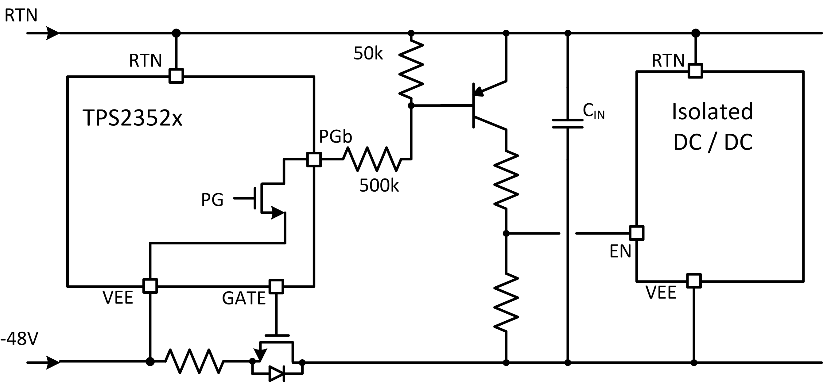
9.2.2.10 Power Good Interface to Downstream DC/DC
It's critical to keep the downstream DC/DC off while the hot swap is charging the bulk capacitor. This can be accomplished through the PGb pin. Note that the VEE of the hot swap and the DC/DC are different and the Power Good can not be directly tied to the EN or UV of the DC/DC. The application circuit below provides a simple way to control the downstream converter with the PGb pin of the hot swap.
 Figure 16. Interface to DC/DC