ZHCSBG7B JULY 2013 – December 2014 TPL5000
PRODUCTION DATA.
6 Pin Configuration and Functions
10-Lead
VSSOP
Top View
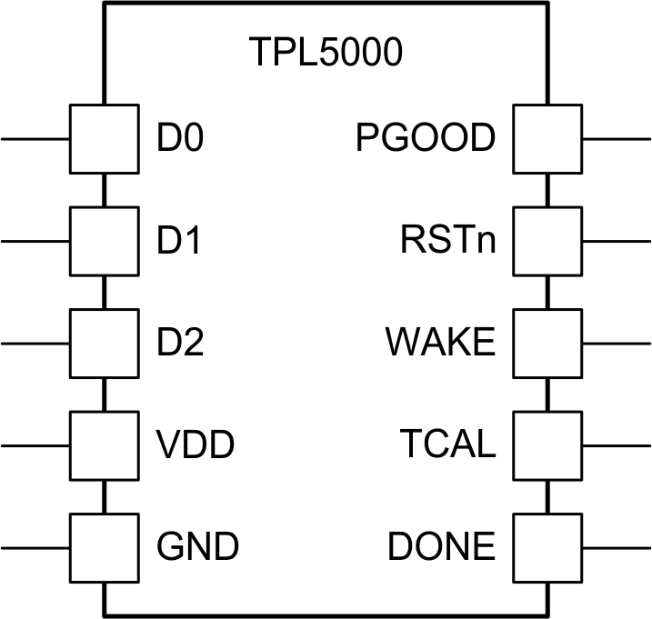
Pin Functions
| PIN | DESCRIPTION | APPLICATION INFORMATION | |
|---|---|---|---|
| NAME | NO. | ||
| D0 | 1 | Logic Input to set period delay (tDP) | Connect to either GND (low logic value) or VDD (high logic value) |
| D1 | 2 | Logic Input to set period delay (tDP) | Connect to either GND (low logic value) or VDD (high logic value) |
| D2 | 3 | Logic Input to set period delay (tDP) | Connect to either GND (low logic value) or VDD (high logic value) |
| VDD | 4 | Supply voltage | |
| GND | 5 | Ground | |
| DONE | 6 | Logic Input for watchdog functionality | |
| TCAL | 7 | Short duration pulse output for estimation of TPL5000 timer delay. | |
| WAKE | 8 | Timer output signal generated every tDP period. | |
| RSTn | 9 | Reset Output (open drain output) | |
| PGOOD | 10 | Digital power good input | |