ZHCSBG7B JULY   2013  – December 2014 TPL5000

PRODUCTION DATA.  

  1. 特性
  2. 应用
  3. 说明
  4. 简化应用电路原理图
  5. 修订历史记录
  6. Pin Configuration and Functions
  7. Specifications
    1. 7.1 Absolute Maximum Ratings
    2. 7.2 ESD Ratings
    3. 7.3 Recommended Operating Ratings
    4. 7.4 Thermal Information
    5. 7.5 Electrical Characteristics
    6. 7.6 Timing Requirements
    7. 7.7 Typical Characteristics
  8. Detailed Description
    1. 8.1 Overview
    2. 8.2 Functional Block Diagram
    3. 8.3 Feature Description
      1. 8.3.1 Supervisor Feature
        1. 8.3.1.1 Calibration Pulse
        2. 8.3.1.2 Overview of the Timing Signals: WAKE, RSTN, TCAL and DONE
        3. 8.3.1.3 Watchdog Feature
        4. 8.3.1.4 Different Utilizations of the TPL5000
      2. 8.3.2 Configuration and Interface
    4. 8.4 Device Functional Modes
  9. Application and Implementation
    1. 9.1 Application Information
    2. 9.2 Typical Application
      1. 9.2.1 Design Requirements
      2. 9.2.2 Detailed Design Procedure
      3. 9.2.3 Application Curve
  10. 10Power Supply Recommendations
  11. 11Layout
    1. 11.1 Layout Guidelines
    2. 11.2 Layout Example
  12. 12器件和文档支持
    1. 12.1 商标
    2. 12.2 静电放电警告
    3. 12.3 术语表
  13. 13机械封装和可订购信息

封装选项

机械数据 (封装 | 引脚)
散热焊盘机械数据 (封装 | 引脚)
订购信息

11 Layout

11.1 Layout Guidelines

The more sensitive pins of the TPL5000 are the digital input pins D0, D1, D2 to select the timer interval. It is mandatory to connect them to VDD or GND through short traces avoiding series resistance. It is mandatory to keep these pins far from traces of high frequency signals, such as clock or communication bus. Signal integrity of WAKE, RSTn and TCAL signal is achieved reducing parasitic capacitance on the traces between the TPL5000 and the micro-controller. In the application where the watchdog feature is not used, the DONE pin is required to be tied to TCAL pin.

11.2 Layout Example

LAYOUT.gif
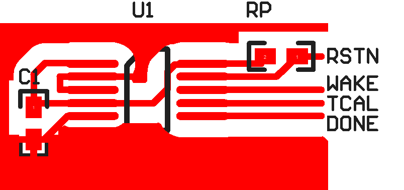
Figure 10. PCB Layout