ZHCSEG2 December 2015 TPIC2040
PRODUCTION DATA.
- 1 特性
- 2 应用
- 3 说明
- 4 修订历史记录
- 5 说明(续)
- 6 Pin Configuration and Functions
-
7 Specifications
- 7.1 Absolute Maximum Ratings
- 7.2 ESD Ratings
- 7.3 Recommended Operating Conditions
- 7.4 Thermal Information
- 7.5 Electrical Characteristics - Common Part
- 7.6 Electrical Characteristics - Charge Pump
- 7.7 Electrical Characteristics - LDO Pre Driver Part
- 7.8 Electrical Characteristics - Spindle Motor Driver Part
- 7.9 Electrical Characteristics - Sled Motor Driver Part
- 7.10 Electrical Characteristics - Focus/ Tilt/Tracking/Driver Part
- 7.11 Electrical Characteristics - Load Driver Part
- 7.12 Electrical Characteristics - Current Switch Part
- 7.13 Electrical Characteristics - Actuator Protection
- 7.14 Electrical Characteristics - Serial Port Voltage Levels
- 7.15 Serial Port I/F Write Timing Requirements
- 7.16 Serial I/F Read Timing Requirements
- 7.17 Typical Characteristics
-
8 Detailed Description
- 8.1 Overview
- 8.2 Functional Block Diagram
- 8.3 Feature Description
- 8.4 Device Functional Modes
- 8.5 Programming
- 8.6
Register Maps
- 8.6.1 Register State Transition
- 8.6.2 DAC Register (12-Bit Write Only)
- 8.6.3 Control Register
- 8.6.4
Detailed Description of Registers
- 8.6.4.1 REG01 12bit DAC for Tilt (VDAC_MAPSW = 0)
- 8.6.4.2 REG02 12bit DAC for Focus (VDAC_MAPSW = 0)
- 8.6.4.3 REG03 12bit DAC for Tracking (VDAC_MAPSW = 0)
- 8.6.4.4 REG04 10bit DAC for Sled1 (VDAC_MAPSW = 0)
- 8.6.4.5 REG05 10bit DAC for Sled2 (VDAC_MAPSW = 0)
- 8.6.4.6 REG08 12bit DAC for Spindle (VDAC_MAPSW = 0)
- 8.6.4.7 REG09 12bit DAC for Load (VDAC_MAPSW = 0)
- 8.6.4.8 REG6A 8-Bit Control Register for CSW_OCP (REG6A)
- 8.6.4.9 REG6C 8-Bit Control Register for Parm1 (REG6C)
- 8.6.4.10 REG6F 8-Bit Control Register for MonitorSet (REG6F)
- 8.6.4.11 REG70 8-Bit Control Register for DriverEna (REG70)
- 8.6.4.12 REG71 8-Bit Control Register for FuncEna (REG71)
- 8.6.4.13 REG72 8-Bit Control Register for ACTCfg (REG72)
- 8.6.4.14 REG73 8-Bit Control Register for Parm0 (REG73)
- 8.6.4.15 REG74 8-Bit Control Register for OptSet (REG74)
- 8.6.4.16 REG75 8-Bit Control Register for TSD_TUP (REG75)
- 8.6.4.17 REG76 8-Bit Control Register for WriteEna (REG76)
- 8.6.4.18 REG77 8-Bit Control Register for ClrReg (REG77)
- 8.6.4.19 REG78 8-Bit Control Register for ActTemp (REG78)
- 8.6.4.20 REG79 8-Bit Control Register for UVLOMon (REG79)
- 8.6.4.21 REG7A 8-Bit Control Register for TsdMon (REG7A)
- 8.6.4.22 REG7B 8-Bit Control Register for ProtMon (REG7B)
- 8.6.4.23 REG7E 8-Bit Control Register for Version (REG7E)
- 8.6.4.24 REG7F 8-Bit Control Register for Status (REG7F)
-
9 Application and Implementation
- 9.1
Application Information
- 9.1.1 DAC Type
- 9.1.2 Example of 12-Bit DAC Sampling Rate for FCS/TRK/TLT
- 9.1.3 Digital Input Coding
- 9.1.4 Example Timing of Target Control System
- 9.1.5 Spindle Motor Driver Part
- 9.1.6 Sled Driver Part
- 9.1.7 Load Driver Part
- 9.1.8 Focus/Track/Tilt Driver Part
- 9.1.9 9-V LDO
- 9.1.10 Monitor Signal on GPOUT
- 9.2 Typical Application
- 9.1
Application Information
- 10Power Supply Recommendations
- 11Layout
- 12器件和文档支持
- 13机械、封装和可订购信息
9 Application and Implementation
NOTE
Information in the following applications sections is not part of the TI component specification, and TI does not warrant its accuracy or completeness. TI’s customers are responsible for determining suitability of components for their purposes. Customers should validate and test their design implementation to confirm system functionality.
NOTE
- Operate every driver channel after 5-V power supplied and stable.
- Appropriate capacity of de-coupling capacitor is required enough value of over 10 μF due to reduce influence of PWM switching noise. And the P5V pin needs to connect a filter of 1 μF. It is effective to put bypass capacitor(about 0.1 µF) near Power pin (P5V_1, P5V_2, P5V_SPM) for PWM switching noise reduction on power and GND line.
- Much current flow to driver circuits, to consider as below matters.
- Pattern-layout, line-impedance, and noise influence from supply line.
9.1 Application Information
9.1.1 DAC Type
TPIC2040 has seven channels of Actuator. Each channel is assigned to the most suitable DAC engine with a different type respectively. ACT(F/T/Ti) has 12-bit DAC. Upper 8 (MSB sign bit) are converted at a time in 5MHz and LSB 4 bits are output in sequence with 1.25-MHz PWM. SPIN, SLED and Load DAC has same DAC types and sampling rate with 312 kHz. All channel except SLED have x6 gain. Table 32 shows configuration of each actuator.
Table 32. DAC Type
| FCS/TRK/TLT | SLED | SPIN | LOAD | |
|---|---|---|---|---|
| Resolution | 12 bit | 10 bit | 12 bit | 12 bit |
| Type | 8-bit oversampling | 10-bit voltage | 8-bit Oversampling | 8-bit Oversampling |
| Sampling | 1.25M / 10bit 312K / 12bit |
312K | 312K | |
| PWM frequency | 312 kHz | About 156 kHz(variable) | 156 kHz | 312 kHz |
| Out range | ±6 V | ±440 mA | ±6 V | ±6 V |
| Feed back | Voltage feedback | Current feedback | Power supply compensation | Voltage feedback Shared with TRK |
9.1.2 Example of 12-Bit DAC Sampling Rate for FCS/TRK/TLT
The input data is separated in the upper 8bits and the lower 4bits. Upper 8bits (MSB sign 1bit) will be put into 8bit current DAC in every 5 MHz. The lower 4bits will be put into one bit current DAC in sequence from upper to lower bit. This one bit DAC output with PWM in 1.25 MHz. At any PWM duty, 100%, 75%, 50%, 25% or 0%, will be summed in 8bit current DAC in every 1.25 MHz. Thus it takes 3.2 µs for all lower 4bits summing to PWM output. As a result, 12-bit data is sampled in every PWM cycle. Example of sampling rate for FCS/TRK/TLT is Figure 44.
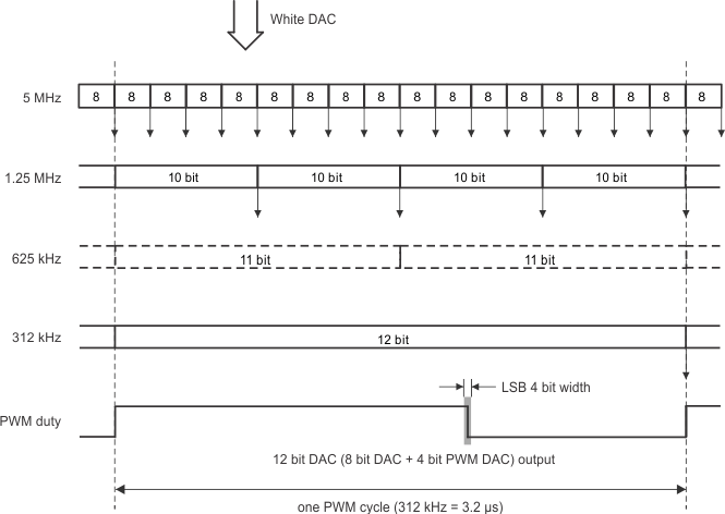 Figure 44. Example of 12-Bit DAC Conversion Time (FCS/TRK/TLT)
9.1.3 Digital Input Coding
The output voltage (current) is commanded via programming to the DAC. All of the DAC input format is 12bit in two’s complement though some DAC has a low resolution. When 12 bits data is input 8 bits DAC, TPIC2040 recognizes four subordinate position bits (LSB) as 0. To arrange for 12-bit DAC format, DSP should shift 8bit or 10 bit data to an appropriate bit position. The full scale is ±1.0 V and driver gain is set 6. The output voltage (Vout) is given by the following equation:


where
- bit[11:0] is the digital input value, range 000000000000b to 111111111111b.
Table 33. DAC Format
| MSB DIGITAL INPUT (BIN) LSB | HEX | DEC | VDAC | ANALOG OUTPUT |
|---|---|---|---|---|
| 1000_0000_0000 | 0x800 | -2048 | -0.9995 | -5.997 |
| 1000_0000_0001 | 0x801 | -2047 | -0.9995 | -5.997 |
| 1111_1111_1111 | 0xFFF | -1 | -0.0005 | -0.003 |
| 0000_0000_0000 | 0x000 | 0 | 0 | 0.000 |
| 0000_0000_0001 | 0x001 | +1 | +0.0005 | +0.003 |
| 0111_1111_1110 | 0x7FE | +2046 | +0.9990 | +5.994 |
| 0111_1111_1111 | 0x7FF | +2047 | +0.9995 | +5.997 |
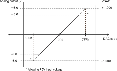 Figure 45. Output Voltage vs DAC Code
9.1.4 Example Timing of Target Control System
TPIC2040 is designed for that meets the requirements updating control data in 400 kHz. The example of control system parameter is listed in Table 34. It takes 0.51 µs for transmit a 16bit data packet to TPIC2040 with 35MHz SCLK. Therefore, DSP can be sent four packets a 400-kHz interval. If SCLK is lower than 28.8MHz, it is required reducing packet quantity under three. For example, Focus/Truck command is updating in every 2.5 µs (400 kHz), and it is able to send another two kind of packet in this same slot. Figure 10 Example DAC control shows the example of the control timing when TPIC2040 is used.
Table 34. Example Timing of Target Control System
| SIGNAL | BIT | UPDATE CYCLE (kHz) |
|---|---|---|
| Focus | 12 | 400 |
| Track | 12 | 400 |
| Tilt | 12 | 200 |
| Sled1 | 10 | 100 |
| Sled2 | 10 | 100 |
| Spindle | 12 | 100 |
| Load | 12 | — |
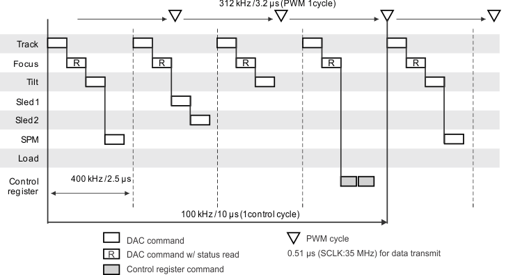 Figure 46. Example DAC Control
9.1.5 Spindle Motor Driver Part
When VSPM is set a positive DAC code then it will be into acceleration mode. IS mode operates then the start-up circuit offers the special start-up pattern sequence to the driver in start-up, and then switches to spin-up mode by detecting the rotor position by BEMF signal from the spindle motor coil.
The spin-down and brake function also be controlled by VSPM DAC value. When it is set the brake command to VSPM, driver goes into active-brake mode, then switch to short-brake mode in slow revolution speed, and then stop automatically. The FG signal is composed from EXOR of three-phase signal, and is output from XFG pin as shown in Figure 47.
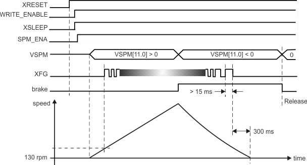 Figure 47. Spindle Operating Sequence
- TI recommends to use down-edge of FG signal for monitoring FG frequency. The FG terminal needs to be pulled up to the appropriate supply voltage by external resistor.
- Short brake mode is asserted after 300 ms of FG signal stays L-level in deceleration.
- The FG output is set to H-level in sleep mode in order to reduce sleep mode current.
- This value is the nominal number of using motor with 16-poles.
- First of all, power supply voltage of P5V must be supplied before any signals input.
9.1.5.1 Spindle PWM Control
The output PWM duty of Spindle is controlled by DAC code (VSPM). The gain in acceleration setting is always six times. However, the maximum output is restricted to P5V_SPM voltage. A dead band which output = 0 exists in the width of plus or minus 0x52 focusing on zero.
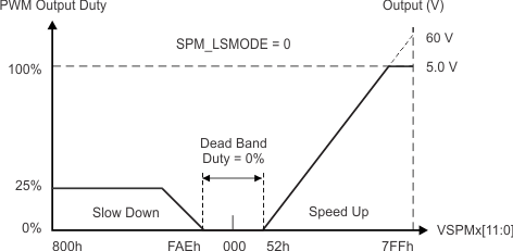 Figure 48. Spindle PWM Control
9.1.5.2 Auto Short Brake Function
TPIC2040 provides auto short brake function which is selecting brake mode automatically by motor speed.
Auto Short Brake is the intelligent brake function that includes two modes: short brake and active brake.
When VSPM value is controlled more than equivalent 75% duty brake, deceleration is done by short brake under the rotation speed is over 3000 rpm. After deceleration, driver goes into Active-brake mode automatically by internal logic circuit under rotation speed is lower 2000 rpm. This function enables low power consumption and silent during braking.
Table 35. Brake Mode
| VSPM[11:0] | ROTATION SPEED (RPM) | |
|---|---|---|
| ABOUT 0 TO 2000 | ABOUT 3000 | |
| 0x000 - 0xFAE | 2-phase short brake | 2-phase short brake |
| 0xFAE - 0xA00 | Active brake | Active brake |
| 0xA00 - 0x800 | Active brake | 3-phase short brake |
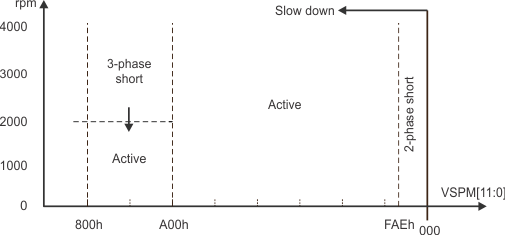 Figure 49. Brake Mode Selections
This value is the nominal number of using motor with 16-poles motor.
9.1.5.3 Spindle Low-Speed Mode
LS mode is the low rotation mode which made the maximum 25% duty. When using SPM_LSMODE = 1, brake mode is always short brake. Figure 50 shows the output duty of LS mode.
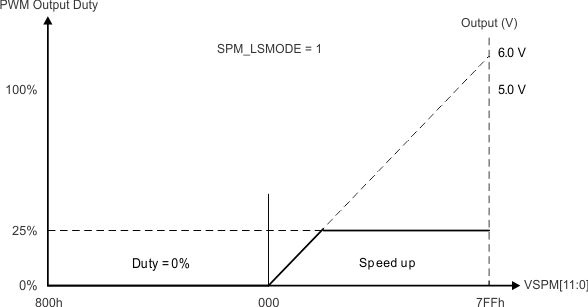 Figure 50. Spindle PWM Control (Low-Speed Mode)
9.1.5.4 Spindle Driver Current Limit Circuit
This IC builds in the SPM current sense resistor which can select resistor value.
The spindle current limit circuit monitors motor current which flows through this resistance, and limits the output current by reducing PWM duty when detecting over current conditions. Table 36 shows resistor value.
A limit current value can be calculated from following formulas.
Table 36. SPM Current Sense Resistor
| SPM_RCOM_SEL[1:0] | RESISTOR VALUE (Ω) | LIMIT CURRENT (mA) |
|---|---|---|
| 00 | 0.22 | 890 |
| 01 | 0.20 | 980 |
| 10 | 0.27 | 725 |
| 11 | 0.25 | 784 |
9.1.6 Sled Driver Part
9.1.6.1 Sled Channel Input versus Output PWM Duty
The Sled driver outputs the PWM pulse set as DAC code (VSLDx) with current feed back. The maximum output is restricted to 440 mA at 0x7FF and 0x800. A dead band which output = 0 exists in the width of plus or minus focusing on zero.
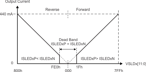 Figure 51. Sled Output Current
- Both outputs of SLED1/2 are L when input code is in dead band.
9.1.6.2 Sled End Detect Function
This device has the function of end position detection for Sled. By this function aim to eliminate the position switch at PUH inner. When this function is enabled, internal logic will detect the sled out zero-cross point and at that time, internal BEMF detect circuit measures the BEMF level of stepping motor. There are six threshold levels. If BEMF is lower than selected threshold, device recognizes motor at stop and ENDDET bit to 1. ENDDET bit will be cleared at the BEMF voltage exceed threshold again.
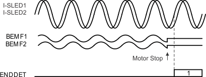 Figure 52. Timing of Sled End Detection
- In order to perform high-precision detection, the sled motor needs to generate higher BEMF voltage. BEMF level depends on the stepping motor characteristic and its speed.
- BEMF detection level is selectable 22, 46, 82, 105, 125, 145 mV.
If the drive speed changes, the timing which BEMF voltage generates will also change. In TPIC2040, detection window can be adjusted to the optimal value by setting EDET_DELAY parameter. Delay time from the point which polarity reverses and width of detection window are adjustable with EDET_DELAY.
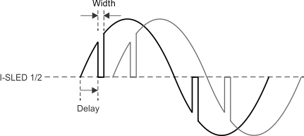 Figure 53. Timing of End Detection Window
9.1.7 Load Driver Part
Load driver outputs the voltage with voltage feedback corresponding to the input DAC value. This channel has power voltage compensation thus it is suit for Slot-in type load control. This channel becomes active exclusively to other actuator channels. Load driver is shared with the TRK driver.
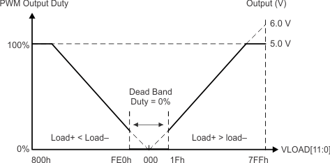 Figure 54. Load Output Duty
- Output voltage is controlled by PWM
- Both LOAD+ and LOAD– are connected to PGND through the internal clamp diode respectively.
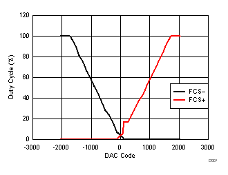
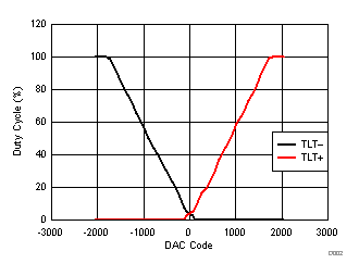
9.1.8 Focus/Track/Tilt Driver Part
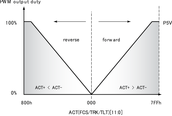 Figure 55. FCS/TRK/TLT Output Duty
9.1.8.1 Differential Tilt Mode
TPIC2040 support differential Tilt mode which output the value calculated from Focus and Tilt. Focus and Tilt can be set in differential mode by DIFF_TLT (REG74) = 1. Because Focus and Tilt are updated at the same time, the update interval of Tilt can be thinned out. Output data changes at after writing VFCS data. Therefore it is necessary to write VFCS data when set VTLT. In differential mode, the output value is calculated as follows.
9.1.9 9-V LDO
TPIC2040 built in function a pre-driver for LDO. The required voltage beyond 1.2 V can be outputted on N-channel FET by choosing external resistance. Arbitrary current can be supplied by selecting the external N-channel FET according to required current capacity. LIN3VG output (= N-channel FET gate control) is controlled to Feedback voltage LINFB is set as 1.215 V. The 22-nF capacitor for phase compensation is certainly installed. And the division resistance for FB is chosen so that it may become less than 3K in total. The example of external components shows Figure 56. The accuracy of output voltage depends for tolerance of resistance.
When not using LDO, it should be open LIN3VG and LINFB should be connected to 3.3 V with LIN3P3_DIS = 1.
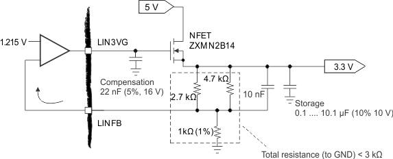 Figure 56. Example Circuit of 3.3-V LDO
9.1.10 Monitor Signal on GPOUT
Able to output a specific signal to GPOUT pin. In order to output a signal, set a signal from REG6F by enabling first and then enable GPOUT_ENA. When two or more signals are set for GPOUT, an output is as logical sum.
It is required to set both LIN3P3_DIS and GPOUT_ENA to 1.
9.2 Typical Application
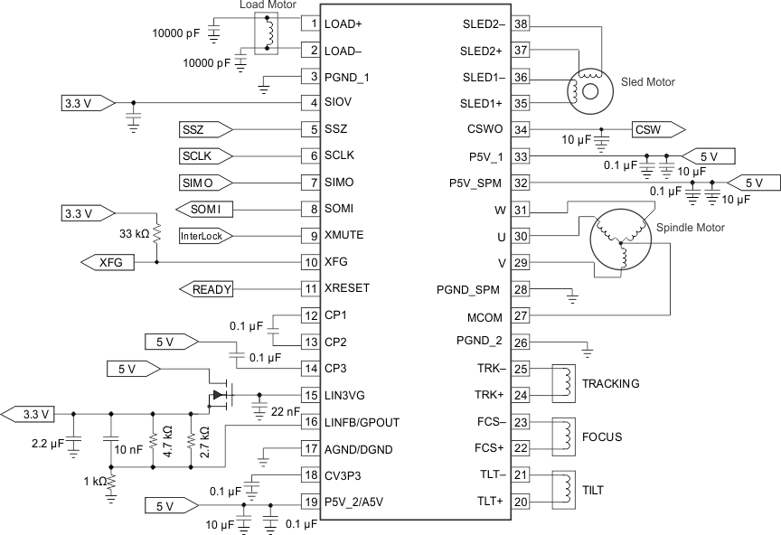 Figure 57. Example of Application Circuit
Table 37. Pin Connection When Specific Function is not Applied
| FUNCTION | PIN | NUMBER | CONNECTION |
|---|---|---|---|
| LDO | LIN3VG | 15 | Open |
| LINFB | 16 | 3.3 V (SIOV) |
9.2.1 Design Requirements
To begin the design process, determine the following:
- Motor configuration: The user can use all motor channels or some of them.
- Power up devices with a 5-V supply.
9.2.2 Detailed Design Procedure
After power up on 5-V supply, the following values may be written to the following registers to enable motors.
- Set WRITE_ENABLE = 1 on REG76 via SPI.
- Set XSLEEP = 1 at REG70
- Enable motor channel by ENA_XXX bits on REG70
- Change the DAC settings for each motor in REG01-0B. Then, output channels will start driving load.
Table 38. Recommended External Components
| PIN | TO | FUNCTION | VALUE (RATE) | UNIT |
|---|---|---|---|---|
| P5V_1 | PGND | Noise decoupling | 10.0 (10%16 V) | μF |
| P5V_2 | PGND | Noise decoupling | 10.0 (10%16 V) | μF |
| P5V_SPM | PGND | Noise decoupling | 10.0 (10%16 V) | μF |
| SIOV | PGND | Noise decoupling | 1.0 (10%10 V) | μF |
| LOAD_P | PGND | Prevent surge current | 10000(10% 16 V) | pF |
| LOAD_N | PGND | Prevent surge current | 10000(10% 16 V) | pF |
| CP1 | CP2 | Charge pump capacitor | 0.1 (10% 16 V) | µF |
| CP3 | P5V | Charge pump capacitor (P5V only, prohibit other power supply) | 0.1 (10% 16 V) | µF |
9.2.3 Application Curves
