ZHCSF88A May 2016 – July 2016 TPD1E1B04
PRODUCTION DATA.
8 Application and Implementation
NOTE
Information in the following applications sections is not part of the TI component specification, and TI does not warrant its accuracy or completeness. TI’s customers are responsible for determining suitability of components for their purposes. Customers should validate and test their design implementation to confirm system functionality.
8.1 Application Information
The TPD1E1B04 is a diode type TVS which is used to provide a path to ground for dissipating ESD events on high-speed signal lines between a human interface connector and a system. As the current from ESD passes through the TVS, only a small voltage drop is present across the diode. This is the voltage presented to the protected IC. The low RDYN of the triggered TVS holds this voltage, VCLAMP, to a safe level for the protected IC.
8.2 Typical Application
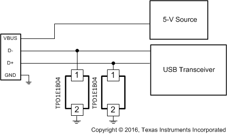
 Figure 11. USB 2.0 ESD Schematic
8.2.1 Design Requirements
For this design example, two TPD1E1B04 devices are being used in a USB 2.0 application. This provides a complete ESD protection scheme.
Given the USB 2.0 application, the parameters listed in Table 1 are known.
Table 1. Design Parameters
| DESIGN PARAMETER | VALUE |
|---|---|
| Signal range on DP-DM lines | 0 V to 3.6 V |
| Operating frequency on DP-DM lines | up to 240 MHz |
8.2.2 Detailed Design Procedure
8.2.2.1 Signal Range
The TPD1E1B04 supports signal ranges between –3.6 V and 3.6 V, which supports the USB 2.0 signal pair on the USB 2.0 application.
8.2.2.2 Operating Frequency
The TPD1E1B04 has a 1-pF (typical) capacitance, which supports the USB 2.0 data rates of 480 Mbps.
8.2.3 Application Curve
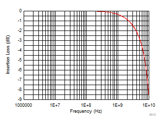
 Figure 12. Insertion Loss