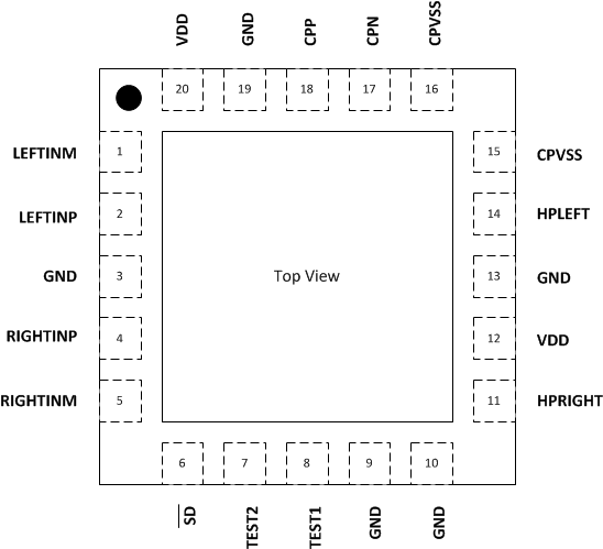
| LEFTINM |
1 |
I |
Left channel negative differential input. Impedance must be matched to LEFTINP. Connect the left input to LEFTINM when using single-ended inputs. |
| LEFTINP |
2 |
I |
Left channel positive differential input. Impedance must be matched to LEFTINM. AC ground LEFTINP near signal source while maintaining matched impedance to LEFTINM when using single-ended inputs. |
| RIGHTINP |
4 |
I |
Right channel positive differential input. Impedance must be matched to RIGHTINM. AC ground RIGHTINP near signal source while maintaining matched impedance to RIGHTINM when using single-ended inputs. |
| GND |
3, 9, 10, 13 |
P |
Analog ground. Must be connected to common supply GND. It is recommended that this pin be used to decouple VDD for analog. Use pin 13 to decouple pin 12 on the QFN package. |
| RIGHTINM |
5 |
I |
Right channel negative differential input. Impedance must be matched to RIGHTINP. Connect the right input to RIGHTINM when using single-ended inputs. |
| SD |
6 |
I |
Shutdown. Active low logic. 5V tolerant input. |
| TEST2 |
7 |
I |
Factory test pins. Pull up to VDD supply. See Applications Diagram. |
| TEST1 |
8 |
I |
Factory test pins. Pull up to VDD supply. See Applications Diagram. |
| HPRIGHT |
11 |
O |
Headphone light channel output. Connect to the right terminal of the headphone jack. |
| VDD |
12 |
P |
Analog VDD. VDD must be connected to common VDD supply. Decouple with its own 1-μF capacitor to analog ground (pin 13). |
| HPLEFT |
14 |
O |
Headphone left channel output. Connect to left terminal of headphone jack. |
| CPVSS |
15, 16 |
P |
Negative supply generated by the charge pump. Decouple to pin 19 or a GND plane. Use a 1 μF capacitor. |
| CPN |
17 |
P |
Charge pump flying capacitor negative terminal. Connect one side of the flying capacitor to CPN. |
| CPP |
18 |
P |
Charge pump flying capacitor positive terminal. Connect one side of the flying capacitor to CPP. |
| GND |
19 |
P |
Charge pump ground. GND must be connected to common supply GND. It is recommended that this pin be decoupled to the VDD of the charge pump pin (pin 20 on the QFN). |
| VDD |
20 |
P |
Charge pump voltage supply. VDD must be connected to the common VDD voltage supply. Decouple to GND (pin 19 ) with its own 1 μF capacitor. |
| Thermal pad |
Die Pad |
P |
Solder the thermal pad on the bottom of the QFN package to the GND plane of the PCB. It is required for mechanical stability and will enhance thermal performance. |