ZHCSH28B September   2017  – December 2017 TPA3221

PRODUCTION DATA.  

  1. 特性
  2. 应用
  3. 说明
    1.     简化原理图
  4. 修订历史记录
  5. Device Comparison Table
  6. Pin Configuration and Functions
    1.     Pin Functions
  7. Specifications
    1. 7.1 Absolute Maximum Ratings
    2. 7.2 ESD Ratings
    3. 7.3 Recommended Operating Conditions
    4. 7.4 Thermal Information
    5. 7.5 Electrical Characteristics
    6. 7.6 Audio Characteristics (BTL)
    7. 7.7 Audio Characteristics (PBTL)
    8. 7.8 Typical Characteristics, BTL Configuration, AD-mode
    9. 7.9 Typical Characteristics, PBTL Configuration, AD-mode
  8. Parameter Measurement Information
  9. Detailed Description
    1. 9.1 Overview
    2. 9.2 Functional Block Diagrams
    3. 9.3 Feature Description
      1. 9.3.1 Internal LDO
        1. 9.3.1.1 Input Configuration, Gain Setting And Master / Slave Operation
      2. 9.3.2 Gain Setting And Master / Slave Operation
      3. 9.3.3 AD-Mode and HEAD-Mode PWM Modulation
      4. 9.3.4 Oscillator
      5. 9.3.5 Input Impedance
      6. 9.3.6 Error Reporting
    4. 9.4 Device Functional Modes
      1. 9.4.1 Powering Up
        1. 9.4.1.1 Startup Ramp Time
      2. 9.4.2 Powering Down
        1. 9.4.2.1 Power Down Ramp Time
      3. 9.4.3 Device Reset
      4. 9.4.4 Device Soft Mute
      5. 9.4.5 Device Protection System
        1. 9.4.5.1 Overload and Short Circuit Current Protection
        2. 9.4.5.2 Signal Clipping and Pulse Injector
        3. 9.4.5.3 DC Speaker Protection
        4. 9.4.5.4 Pin-to-Pin Short Circuit Protection (PPSC)
        5. 9.4.5.5 Overtemperature Protection OTW and OTE
        6. 9.4.5.6 Undervoltage Protection (UVP), Overvoltage Protection (OVP) and Power-on Reset (POR)
        7. 9.4.5.7 Fault Handling
  10. 10Application and Implementation
    1. 10.1 Application Information
    2. 10.2 Typical Applications
      1. 10.2.1 Stereo BTL Application
        1. 10.2.1.1 Design Requirements
        2. 10.2.1.2 Detailed Design Procedures
          1. 10.2.1.2.1 Decoupling Capacitor Recommendations
          2. 10.2.1.2.2 PVDD Capacitor Recommendation
          3. 10.2.1.2.3 BST capacitors
          4. 10.2.1.2.4 PCB Material Recommendation
      2. 10.2.2 Typical Application, Differential (2N), AD-Mode PBTL (Outputs Paralleled before LC filter)
        1. 10.2.2.1 Design Requirements
      3. 10.2.3 Typical Application, Differential (2N), AD-Mode PBTL (Outputs Paralleled after LC filter)
        1. 10.2.3.1 Design Requirements
  11. 11Power Supply Recommendations
    1. 11.1 Power Supplies
      1. 11.1.1 VDD Supply
      2. 11.1.2 AVDD and GVDD Supplies
      3. 11.1.3 PVDD Supply
      4. 11.1.4 BST Supply
  12. 12Layout
    1. 12.1 Layout Guidelines
    2. 12.2 Layout Examples
      1. 12.2.1 BTL Application Printed Circuit Board Layout Example
      2. 12.2.2 PBTL (Outputs Paralleled before LC filter) Application Printed Circuit Board Layout Example
      3. 12.2.3 PBTL (Outputs Paralleled after LC filter) Application Printed Circuit Board Layout Example
  13. 13器件和文档支持
    1. 13.1 文档支持
    2. 13.2 接收文档更新通知
    3. 13.3 社区资源
    4. 13.4 商标
    5. 13.5 静电放电警告
    6. 13.6 Glossary
  14. 14机械、封装和可订购信息

封装选项

机械数据 (封装 | 引脚)
散热焊盘机械数据 (封装 | 引脚)
订购信息

Typical Application, Differential (2N), AD-Mode PBTL (Outputs Paralleled before LC filter)

TPA3221 can be configured in mono PBTL mode by paralleling the outputs before the LC filter or after the LC filter (see Typical Application, Differential (2N), AD-Mode PBTL (Outputs Paralleled after LC filter)). Paralleled outputs before the LC filter is recommended for better performance and limiting the number of output LC filter inductors.
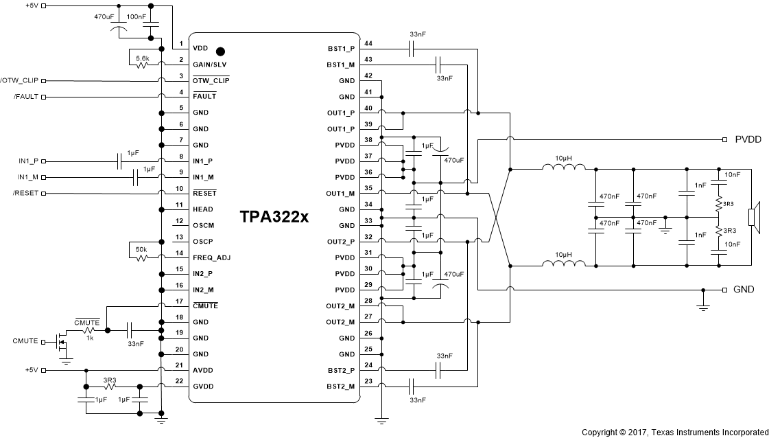
TPA3221 TypAppPrePBTL_slasee9.gifFigure 51. Typical Differential (2N) AD-Mode PBTL Application