ZHCSH28B September 2017 – December 2017 TPA3221
PRODUCTION DATA.
- 1 特性
- 2 应用
- 3 说明
- 4 修订历史记录
- 5 Device Comparison Table
- 6 Pin Configuration and Functions
-
7 Specifications
- 7.1 Absolute Maximum Ratings
- 7.2 ESD Ratings
- 7.3 Recommended Operating Conditions
- 7.4 Thermal Information
- 7.5 Electrical Characteristics
- 7.6 Audio Characteristics (BTL)
- 7.7 Audio Characteristics (PBTL)
- 7.8 Typical Characteristics, BTL Configuration, AD-mode
- 7.9 Typical Characteristics, PBTL Configuration, AD-mode
- 8 Parameter Measurement Information
-
9 Detailed Description
- 9.1 Overview
- 9.2 Functional Block Diagrams
- 9.3 Feature Description
- 9.4
Device Functional Modes
- 9.4.1 Powering Up
- 9.4.2 Powering Down
- 9.4.3 Device Reset
- 9.4.4 Device Soft Mute
- 9.4.5
Device Protection System
- 9.4.5.1 Overload and Short Circuit Current Protection
- 9.4.5.2 Signal Clipping and Pulse Injector
- 9.4.5.3 DC Speaker Protection
- 9.4.5.4 Pin-to-Pin Short Circuit Protection (PPSC)
- 9.4.5.5 Overtemperature Protection OTW and OTE
- 9.4.5.6 Undervoltage Protection (UVP), Overvoltage Protection (OVP) and Power-on Reset (POR)
- 9.4.5.7 Fault Handling
- 10Application and Implementation
- 11Power Supply Recommendations
- 12Layout
- 13器件和文档支持
- 14机械、封装和可订购信息
9.3.1 Internal LDO
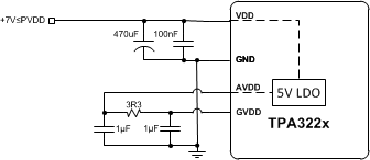
TPA3221 has a built in optional LDO (Low dropout voltage regulator) to supply the analog and digital circuits as well as the gate drive for the output stages. The LDO can be used in systems where only the high voltage power rail is available, hence no additional power supply rails need to be generated for the TPA3221 to operate. As being a linear regulator, the LDO will add to the power losses of the device due to the (PVDD-5V) voltage drop and the supply current for AVDD and GVDD given in the Electrical Characteristics table.
 Figure 28. Internal LDO for Single Supply Systems
When using the internal LDO in TPA3221 the VDD terminal should be connected to a voltage source between 7V and PVDD. In a single supply system the VDD terminal should be connected directly to the PVDD terminal. The LDO output is connected to the AVDD terminal, and can be used to supply the gate drive by supplying the GVDD from AVDD through a RC filter for best noise performance as shown in Figure 28.
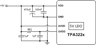
 Figure 29. Internal LDO Bypass for Highest Power Efficiency
For highest system power efficiency the LDO can be bypassed by connecting VDD to an external 5 V supply. In this configuration AVDD and GVDD should be supplied by 5 V from the external power supply. GVDD should be supplied through a RC filter for best noise performance as shown in Figure 29.