ZHCSKH3 November   2019 TMP392

PRODUCTION DATA.  

  1. 特性
  2. 应用
  3. 说明
    1.     简化原理图
  4. 修订历史记录
  5. Pin Configuration and Functions
    1.     Pin Functions
  6. Specifications
    1. 6.1 Absolute Maximum Ratings
    2. 6.2 ESD Ratings
    3. 6.3 Recommended Operating Conditions
    4. 6.4 Thermal Information
    5. 6.5 Electrical Characteristics
    6. 6.6 Typical Characteristics
  7. Detailed Description
    1. 7.1 Overview
    2. 7.2 Functional Block Diagram
    3. 7.3 Feature Description
      1. 7.3.1 TMP392 Programming Tables
      2. 7.3.2 Trip Test
      3. 7.3.3 20°C Hysteresis
    4. 7.4 Device Functional Modes
  8. Application and Implementation
    1. 8.1 Applications Information
    2. 8.2 Typical Applications
      1. 8.2.1 Simplified Application Schematic
        1. 8.2.1.1 Design Requirements
        2. 8.2.1.2 Detailed Design Procedure
        3. 8.2.1.3 Application Curves
      2. 8.2.2 TMP392 With 10°C Hysteresis
        1. 8.2.2.1 Design Requirements
        2. 8.2.2.2 Detailed Design Procedure
        3. 8.2.2.3 Application Curve
      3. 8.2.3 One Channel Operation for Hot Trip Point up to 124°C
        1. 8.2.3.1 Application Curve
      4. 8.2.4 One Channel Operation for Warm Trip Point from 30°C up to 105°C
  9. Power Supply Recommendations
  10. 10Layout
    1. 10.1 Layout Guidelines
    2. 10.2 Layout Example
  11. 11器件和文档支持
    1. 11.1 接收文档更新通知
    2. 11.2 支持资源
    3. 11.3 商标
    4. 11.4 静电放电警告
    5. 11.5 Glossary
  12. 12机械、封装和可订购信息

封装选项

机械数据 (封装 | 引脚)
散热焊盘机械数据 (封装 | 引脚)
订购信息

Trip Test

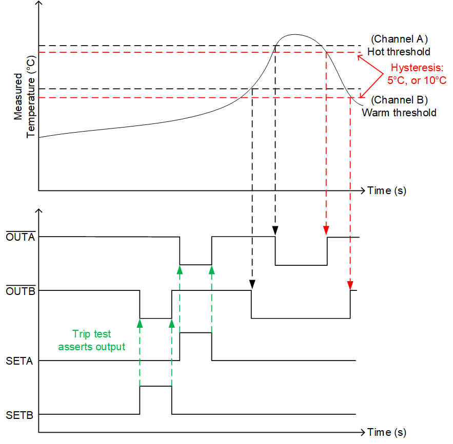
The purpose of the trip test is in system manufacturing test without putting the TMP392 through costly temperature verification of the assembly of TMP392 and pullup resistors. When the SETA or SETB pin is set to a high logic level, the associated output goes low. When the input pin level goes low, the output goes to its previous condition before the trip test. The trip test does not affect the current condition of the device. The trip test signals should stay above 0.8 × VDD for logic high and below 0.2 × VDD for logic low.

The trip test operation is shown in Figure 8. The trip test must be performed with a single toggle when the device is operating at a temperature that will not cause the corresponding output to trip. The trip test is intended for production testing after assembly, and must not be used as a functional feature.
TMP392 TMP392-trip-test-operation-SBOS904.gifFigure 8. TMP392 Trip Test Operation