ZHCSMJ5F june   2010  – december 2020 TLV809

PRODUCTION DATA  

  1. 特性
  2. 应用
  3. 说明
  4. Revision History
  5. Device Comparison
  6. Pin Configuration and Functions
    1.     Pin Functions
  7. Specifications
    1. 7.1 Absolute Maximum Ratings
    2. 7.2 ESD Ratings
    3. 7.3 Recommended Operating Conditions
    4. 7.4 Thermal Information
    5. 7.5 Electrical Characteristics
    6. 7.6 Timing Requirements
    7. 7.7 Switching Characteristics
    8. 7.8 Timing Diagrams
    9. 7.9 Typical Characteristics
  8. Detailed Description
    1. 8.1 Overview
    2. 8.2 Functional Block Diagram
    3. 8.3 Feature Description
      1. 8.3.1 Supply Voltage Monitoring
      2. 8.3.2 RESET Output
    4. 8.4 Device Functional Modes
  9. Application and Implementation
    1. 9.1 Application Information
      1. 9.1.1 VDD Transient Rejection
      2. 9.1.2 Reset During Power-Up and Power-Down
    2. 9.2 Typical Application
      1. 9.2.1 Design Requirements
      2. 9.2.2 Detailed Design Procedure
      3. 9.2.3 Application Curve
  10. 10Power Supply Recommendations
  11. 11Layout
    1. 11.1 Layout Guidelines
    2. 11.2 Layout Example
  12. 12Device and Documentation Support
    1. 12.1 Documentation Support
      1. 12.1.1 Related Documentation
    2. 12.2 支持资源
    3. 12.3 Trademarks
    4. 12.4 静电放电警告
    5. 12.5 术语表
  13. 13Mechanical, Packaging, and Orderable Information

封装选项

机械数据 (封装 | 引脚)
散热焊盘机械数据 (封装 | 引脚)
订购信息

Reset During Power-Up and Power-Down

The device output is valid when VDD is greater than 1.1 V. When VDD is less than 1.1 V, the output transistor turns off and becomes high impedance. The voltage on the RESET pin rises to the voltage level connected to the pullup resistor. Figure 9-2 shows a typical waveform for power-up.
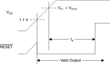
GUID-DA2DF579-0CE5-4372-8734-15B9AC91CB2F-low.gifFigure 9-2 Power-Up Response