ZHCSDR6 May 2015 TLV713P-Q1
PRODUCTION DATA.
10 Layout
10.1 Layout Guidelines
10.1.1 Board Layout Recommendations to Improve PSRR and Noise Performance
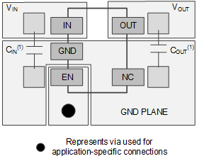
Input and output capacitors must be placed as close to the device pins as possible. To improve ac performance (such as PSRR, output noise, and transient response), TI recommends that the board be designed with separate ground planes for VIN and VOUT, with the ground plane connected only at the device GND pin. In addition, the output capacitor ground connection must be connected directly to the device GND pin. High-ESR capacitors may degrade PSRR performance.
10.2 Layout Example

10.3 Power Dissipation
The ability to remove heat from the die is different for each package type, presenting different considerations in the printed-circuit-board (PCB) layout. The PCB area around the device that is free of other components moves the heat from the device to the ambient air. Performance data for JEDEC low- and high-K boards are given in the table. Using heavier copper increases the effectiveness in removing heat from the device. The addition of plated through-holes to heat-dissipating layers also improves the heatsink effectiveness.
Power dissipation depends on input voltage and load conditions. Power dissipation (PD) can be approximated by the product of the output current times the voltage drop across the output pass element (VIN to VOUT), as shown in Equation 3.
Estimating the junction temperature can be done by using the thermal metrics ΨJT and ΨJB, as discussed in the table. These metrics are a more accurate representation of the heat transfer characteristics of the die and the package than RθJA. The junction temperature can be estimated with Equation 4.

where
- PD is the power dissipation shown by Equation 3,
- TT is the temperature at the center-top of the device package,
- TB is the PCB temperature measured 1 mm away from the device package on the PCB surface.
NOTE
Both TT and TB can be measured on actual application boards using a thermo‐gun (an infrared thermometer).
For more information about measuring TT and TB, see application note Using New Thermal Metrics (SBVA025), available for download at www.ti.com.