ZHCSF07A March 2016 – January 2017 TLV62095
PRODUCTION DATA.
- 1 特性
- 2 应用范围
- 3 说明
- 4 修订历史记录
- 5 Pin Configuration and Functions
- 6 Specifications
- 7 Detailed Description
- 8 Application and Implementation
- 9 Power Supply Recommendations
- 10Layout
- 11器件和文档支持
- 12机械、封装和可订购信息
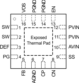
5 Pin Configuration and Functions
16-Pin VQFN with Thermal PAD
RGT
(Top View)

Pin Functions
| PIN | DESCRIPTION | |
|---|---|---|
| NAME | NO. | |
| SW | 1, 2 | Switch pin of the power stage. |
| DEF | 3 | This pin is used for internal logic and needs to be pulled high. This pin must be connected to the AVIN pin. |
| PG | 4 | Power good open drain output. A pull up resistor can not be connected to any voltage higher than the input voltage. |
| FB | 5 | Feedback pin for regulating the output voltage. |
| AGND | 6 | Analog ground. |
| CP | 7 | Internal charge pump's flying capacitor. Connect a 10nF capacitor between CP and CN. |
| CN | 8 | Internal charge pump's flying capacitor. Connect a 10nF capacitor between CP and CN. |
| SS | 9 | Soft-start control pin. A capacitor is connected to this pin and sets the soft startup time. Leaving this pin floating sets the minimum start-up time. |
| AVIN | 10 | Analog supply input voltage pin. |
| PVIN | 11,12 | Power supply input voltage pin. |
| EN | 13 | Enable pin. This pin has an active pull down resistor of typically 400kΩ, which is active when EN is low. To enable the device, this pin needs to be pulled high. Pulling this pin low disables the device. |
| PGND | 14,15 | Power ground. |
| VOS | 16 | Output voltage sense pin. This pin must be directly connected to the output voltage. |
| Exposed Thermal Pad | The exposed thermal pad must be connected to AGND. It must be soldered for mechanical reliability. | |