ZHCS792F March 2012 – January 2017 TLV62090
PRODUCTION DATA.
8 Application and Implementation
NOTE
Information in the following applications sections is not part of the TI component specification, and TI does not warrant its accuracy or completeness. TI’s customers are responsible for determining suitability of components for their purposes. Customers should validate and test their design implementation to confirm system functionality.
8.1 Application Information
The TLV62090 is a 3-A high frequency synchronous step-down converter optimized for small solution size, high efficiency and suitable for battery powered applications.
8.2 Typical Application
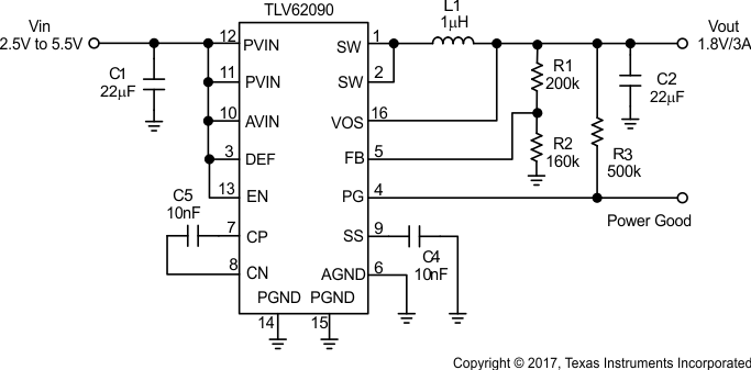 Figure 11. TLV62090 Typical Application Circuit
8.2.1 Design Requirements
The design guideline provides a component selection to operate the device within the recommended operating conditions.
For the typical application example, the following input parameters are used. See Table 2.
Table 2. Design Parameters
| DESIGN PARAMETERS | EXAMPLE VALUES |
|---|---|
| Input Voltage Range | 2.5 V to 5.5 V |
| Output Voltage | 1.8 V |
| Transient Response | ±5% VOUT |
| Input Voltage Ripple | 400 mV |
| Output Voltage Ripple | 30 mV |
| Output current rating | 3 A |
| Operating frequency | 1.4 MHz |
Table 3 shows the list of components for the Application Characteristic Curves.
Table 3. List of Components
8.2.2 Detailed Design Procedure
8.2.2.1 Custom Design with WEBENCH® Tools
Click here to create a custom design using the TLV62090 device with the WEBENCH® Power Designer.
- Start by entering your VIN, VOUT, and IOUT requirements.
- Optimize your design for key parameters like efficiency, footprint and cost using the optimizer dial and compare this design with other possible solutions from Texas Instruments.
- The WEBENCH Power Designer provides you with a customized schematic along with a list of materials with real time pricing and component availability.
- In most cases, you will also be able to:
- Run electrical simulations to see important waveforms and circuit performance
- Run thermal simulations to understand the thermal performance of your board
- Export your customized schematic and layout into popular CAD formats
- Print PDF reports for the design, and share your design with colleagues
- Get more information about WEBENCH tools at www.ti.com/WEBENCH.
The first step is the selection of the output filter components. To simplify this process, Table 4 outlines possible inductor and capacitor value combinations.
Table 4. Output Filter Selection
| INDUCTOR VALUE [µH](3) | OUTPUT CAPACITOR VALUE [µF](2) | ||||
|---|---|---|---|---|---|
| 10 | 22 | 47 | 100 | 150 | |
| 0.47 | √ | √ | √ | √ | |
| 1.0 | √ | √(1) | √ | √ | √ |
| 2.2 | √ | √ | √ | √ | √ |
| 3.3 | |||||
8.2.2.2 Inductor Selection
The inductor selection is affected by several parameters like inductor ripple current, output voltage ripple, transition point into power save mode, and efficiency. See Table 5 for typical inductors.
Table 5. Inductor Selection
| INDUCTOR VALUE | COMPONENT SUPPLIER | SIZE (LxWxH mm) | Isat/DCR (max) |
|---|---|---|---|
| 0.6 µH | Coilcraft XAL4012-601 | 4 x 4 x 2.1 | 7.9A/10.5 mΩ |
| 1 µH | Coilcraft XAL4020-102 | 4 x 4 x 2.1 | 6.7A/14.6 mΩ |
| 1 µH | Coilcraft XFL4020-102 | 4 x 4 x 2.1 | 4.5 A/11.9 mΩ |
| 0.47 µH | TOKO DFE252012CR47 | 2.5 x 2 x 1.2 | 3.7A/39 mΩ |
| 1 µH | TOKO DFE252012C1R0 | 2.5 x 2 x 1.2 | 3.0A/59 mΩ |
| 0.68 µH | TOKO DFE322512CR68 | 3.2 x 2.5 x 1.2 | 3.5A/35 mΩ |
| 1 µH | TOKO DFE322512C1R0 | 3.2 x 2.5 x 1.2 | 3.1A/45 mΩ |
In addition, the inductor has to be rated for the appropriate saturation current and DC resistance (DCR). Equation 5 and Equation 6 calculate the maximum inductor current under static load conditions. The formula takes the converter efficiency into account. The converter efficiency can be taken from the data sheet graphs or 80% can be used as a conservative approach. The calculation must be done for the maximum input voltage where the peak switch current is highest.


where
ƒ = Converter switching frequency (typically 1.4 MHz)
L = Selected inductor value
η = Estimated converter efficiency (use the number from the efficiency curves or 0.80 as a conservative assumption)
Calculating the maximum inductor current using the actual operating conditions gives the minimum saturation current. A margin of about 20% should be added to cover for load transients during operation.
8.2.2.3 Input and Output Capacitor Selection
For best output and input voltage filtering, low ESR (X5R or X7R) ceramic capacitors are recommended. The input capacitor minimizes input voltage ripple, suppresses input voltage spikes and provides a stable system rail for the device. A 22-µF or larger input capacitor is recommended. The output capacitor value can range from 10 µF up to 150 µF and beyond. Load transient testing and measuring the bode plot are good ways to verify stability with larger capacitor values.
The recommended typical output capacitor value is 22 µF (nominal) and can vary over a wide range as outline in the output filter selection table. For output voltages above 1.8 V, noise can cause duty cycle jitter. This does not degrade device performance. Using an output capacitor of 2 x 22 µF (nominal) for output voltages >1.8 V avoids duty cycle jitter.
Ceramic capacitor have a DC-Bias effect, which has a strong influence on the final effective capacitance. Choose the right capacitor carefully in combination with considering its package size and voltage rating.
8.2.2.4 Setting the Output Voltage
The output voltage is set by an external resistor divider according to the following equations:


When sizing R2, in order to achieve low quiescent current and acceptable noise sensitivity, use a minimum of 5 µA for the feedback current IFB. Larger currents through R2 improve noise sensitivity and output voltage accuracy. A feed forward capacitor is not required for proper operation.
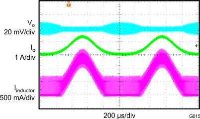
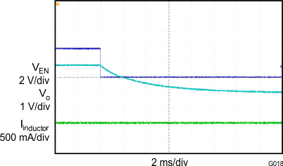
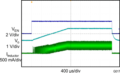
8.2.3 Application Curves
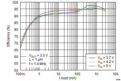
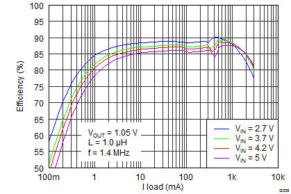
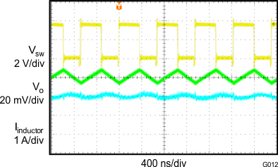
| VIN = 3.7 V | VO = 1.8 V/3 A | f = 1.4 MHz |
| L = 1 µH |
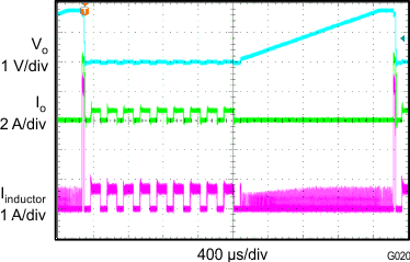
| VIN = 3.7 V | VO = 1.8 V | f = 1.4 MHz |
| L = 1 µH |
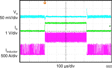
| VIN = 3.7 V | VO = 1.8 V | 20 mA to 1 A | ||
| f = 1.4 MHz | L = 1 µH | CO = 22 µF |
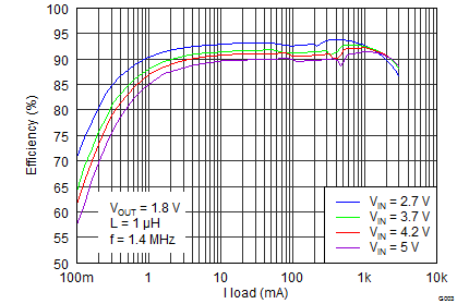
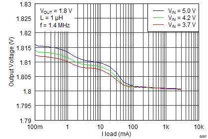
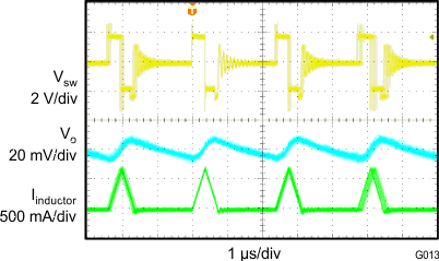
| VIN = 3.7 V | VO = 1.8 V/100 mA | f = 1.4 MHz |
| L = 1 µH |
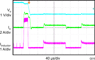
| VIN = 3.7 V | VO = 1.8 V | f = 1.4 MHz |
| L = 1 µH |
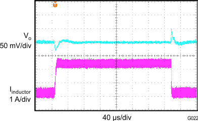
| VIN = 3.7 V | VO = 1.8 V | 0.3 A to 2.5 A |
| f = 1.4 MHz | L = 1 µH | CO = 22 µF |
