ZHCSE67B October   2015  – July 2018 TLV62085

PRODUCTION DATA.  

  1. 特性
  2. 应用
  3. 说明
    1.     Device Images
      1.      典型应用电路原理图
      2.      VIN = 5V 时的效率
  4. 修订历史记录
  5. Pin Configuration and Functions
    1.     Pin Functions
  6. Specifications
    1. 6.1 Absolute Maximum Ratings
    2. 6.2 ESD Ratings
    3. 6.3 Recommended Operating Conditions
    4. 6.4 Thermal Information
    5. 6.5 Electrical Characteristics
    6. 6.6 Typical Characteristics
  7. Detailed Description
    1. 7.1 Overview
    2. 7.2 Functional Block Diagram
    3. 7.3 Feature Description
      1. 7.3.1 Power Save Mode
      2. 7.3.2 100% Duty Cycle Low Dropout Operation
      3. 7.3.3 Soft Start
      4. 7.3.4 Switch Current Limit and Hiccup Short-Circuit Protection
      5. 7.3.5 Undervoltage Lockout
      6. 7.3.6 Thermal Shutdown
    4. 7.4 Device Functional Modes
      1. 7.4.1 Enable and Disable
      2. 7.4.2 Power Good
  8. Application and Implementation
    1. 8.1 Application Information
    2. 8.2 Typical Application
      1. 8.2.1 Design Requirements
      2. 8.2.2 Detailed Design Procedure
        1. 8.2.2.1 Custom Design with WEBENCH® Tools
        2. 8.2.2.2 Setting The Output Voltage
        3. 8.2.2.3 Output Filter Design
        4. 8.2.2.4 Inductor Selection
        5. 8.2.2.5 Capacitor Selection
      3. 8.2.3 Application Curves
  9. Power Supply Recommendations
  10. 10Layout
    1. 10.1 Layout Guidelines
    2. 10.2 Layout Example
    3. 10.3 Thermal Considerations
  11. 11器件和文档支持
    1. 11.1 开发支持
      1. 11.1.1 使用 WEBENCH® 工具定制设计方案
      2. 11.1.2 第三方产品免责声明
    2. 11.2 文档支持
      1. 11.2.1 相关文档
    3. 11.3 接收文档更新通知
    4. 11.4 社区资源
    5. 11.5 商标
    6. 11.6 静电放电警告
    7. 11.7 术语表
  12. 12机械、封装和可订购信息

封装选项

机械数据 (封装 | 引脚)
散热焊盘机械数据 (封装 | 引脚)
订购信息

Power Save Mode

As the load current decreases, the TLV62085 enters Power Save Mode (PSM) operation. During Power Save Mode, the converter operates with reduced switching frequency and with a minimum quiescent current maintaining high efficiency. Power Save Mode occurs when the inductor current becomes discontinuous. Power Save Mode is based on a fixed on-time architecture, as related in Equation 1. The switching frequency over the whole load current range is also shown in Figure 1 for a shown typical application.
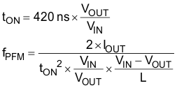
Equation 1. TLV62085 EQ_ton.gif

In PSM, the output voltage rises slightly above the nominal output voltage, as shown in Figure 10. This effect is minimized by increasing the output capacitor or inductor value.

During PAUSE period in PSM (shown in Figure 3), the device does not change the PG pin state nor does it detect an UVLO event, in order to achieve a minimum quiescent current and maintain high efficiency at light loads.

TLV62085 TLV62085_PSM.gifFigure 3. Power Save Mode Waveform Diagram