ZHCSFZ5A February   2017  – December 2017 TLV3201-Q1 , TLV3202-Q1

PRODUCTION DATA.  

  1. 特性
  2. 应用
  3. 说明
    1.     Device Images
      1.      阈值检测器
      2.      传播延迟与过驱动
  4. 修订历史记录
  5. Device Comparison Table
  6. Pin Configuration and Functions
    1.     Pin Functions: TLV3201-Q1
    2.     Pin Functions: TLV3202-Q1
  7. Specifications
    1. 7.1 Absolute Maximum Ratings
    2. 7.2 ESD Ratings
    3. 7.3 Recommended Operating Conditions
    4. 7.4 Thermal Information
    5. 7.5 Electrical Characteristics: VCC = 5 V
    6. 7.6 Electrical Characteristics: VCC = 2.7 V
    7. 7.7 Switching Characteristics
    8. 7.8 Typical Characteristics
  8. Detailed Description
    1. 8.1 Overview
    2. 8.2 Functional Block Diagram
    3. 8.3 Feature Description
      1. 8.3.1 Operating Voltage
      2. 8.3.2 Input Overvoltage Protection
    4. 8.4 Device Functional Modes
  9. Application and Implementation
    1. 9.1 Application Information
      1. 9.1.1 Comparator Inputs
      2. 9.1.2 External Hysteresis
        1. 9.1.2.1 Inverting Comparator with Hysteresis
        2. 9.1.2.2 Noninverting Comparator With Hysteresis
      3. 9.1.3 Capacitive Loads
    2. 9.2 Typical Applications
      1. 9.2.1 TLV3201-Q1 Configured as an AC-Coupled Comparator
        1. 9.2.1.1 Design Requirements
        2. 9.2.1.2 Detailed Design Procedure
        3. 9.2.1.3 Application Curve
      2. 9.2.2 TLV3201-Q1 and OPA320 Configured as a Fast-Response Output Current Monitor
      3. 9.2.3 TLV3201-Q1 and TMP20 Configured as a Precision Analog Temperature Switch
  10. 10Power Supply Recommendations
  11. 11Layout
    1. 11.1 Layout Guidelines
    2. 11.2 Layout Example
  12. 12器件和文档支持
    1. 12.1 器件支持
      1. 12.1.1 开发支持
        1. 12.1.1.1 TINA-TI™ 仿真软件(免费下载)
        2. 12.1.1.2 通用运算放大器评估模块 (EVM)
        3. 12.1.1.3 TI 高精度设计
        4. 12.1.1.4 WEBENCH滤波器设计器
    2. 12.2 文档支持
      1. 12.2.1 相关文档
    3. 12.3 相关链接
    4. 12.4 接收文档更新通知
    5. 12.5 社区资源
    6. 12.6 商标
    7. 12.7 静电放电警告
    8. 12.8 Glossary
  13. 13机械、封装和可订购信息

封装选项

机械数据 (封装 | 引脚)
散热焊盘机械数据 (封装 | 引脚)
订购信息

Typical Characteristics

at TA = 25°C, VCC = 5 V, and input overdrive (VOD) = 20 mV (unless otherwise noted)
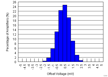
TLV3201-Q1 TLV3202-Q1 Offset Distribution.png
Figure 1. Offset Voltage Distribution
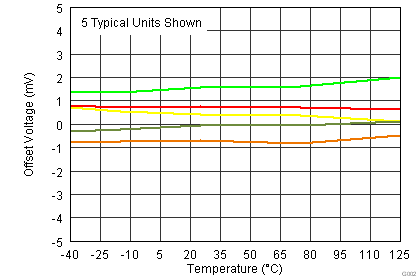
TLV3201-Q1 TLV3202-Q1 Offset vs temperature.png
Figure 3. Offset Voltage vs Temperature
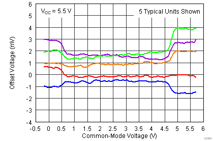
TLV3201-Q1 TLV3202-Q1 Offset vs CMcfg 5_5.png
Figure 5. Offset Voltage vs Common-Mode Voltage
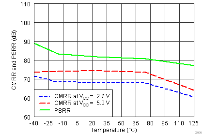
TLV3201-Q1 TLV3202-Q1 CMRR-PSRR vs Temp.png
Figure 7. Common-Mode Rejection Ratio and
Power-Supply Rejection Ratio vs Temperature
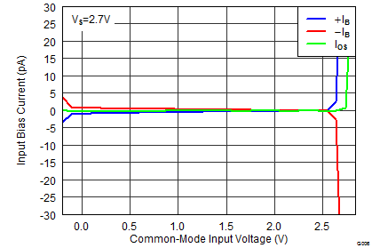
TLV3201-Q1 TLV3202-Q1 IB vs CM 2p5.png
Figure 9. Input Bias Current and Input Offset Current
vs Common-Mode Input Voltage
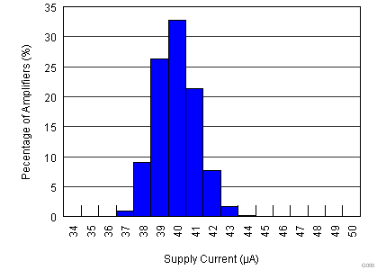
TLV3201-Q1 TLV3202-Q1 IQ Distribution.png
Figure 11. Quiescent Current Distribution
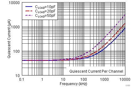
TLV3201-Q1 TLV3202-Q1 IQ vs Fswitch.png
Figure 13. Quiescent Current vs Switching Frequency
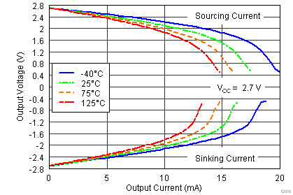
TLV3201-Q1 TLV3202-Q1 IOUT vs Vout 2p7.png
Figure 15. Output Voltage vs Output Current
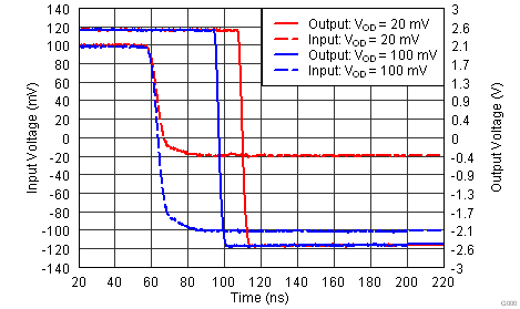
TLV3201-Q1 TLV3202-Q1 Prop Delay HL.png
Figure 17. Propagation Delay Falling Edge
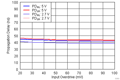
TLV3201-Q1 TLV3202-Q1 tc_3_input_overdrive_vs_prop_delay_bos561.png
Figure 19. Propagation Delay vs Input Overdrive
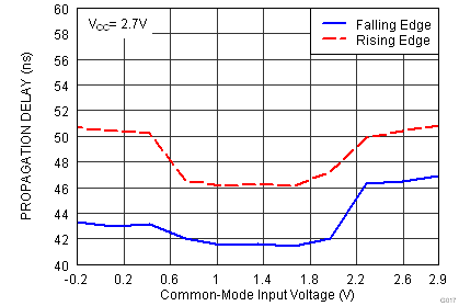
TLV3201-Q1 TLV3202-Q1 Prop vs VCM 2p7.png
Figure 21. Propagation Delay vs Common-Mode Voltage
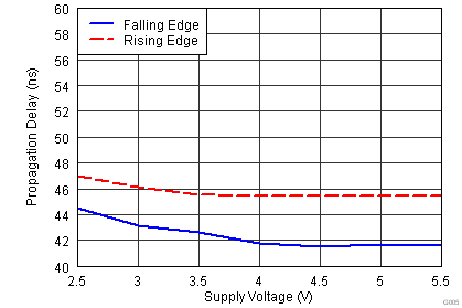
TLV3201-Q1 TLV3202-Q1 tc_5_supply voltage_vs_prop_delay_bos561.png
Figure 23. Propagation Delay vs Supply Voltage
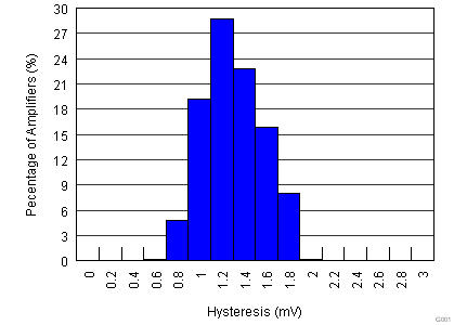
TLV3201-Q1 TLV3202-Q1 Hysteresis Distribution.png
Figure 2. Hysteresis Distribution
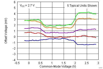
TLV3201-Q1 TLV3202-Q1 Offset vs CMcfg.png
Figure 4. Offset Voltage vs Common-Mode Voltage
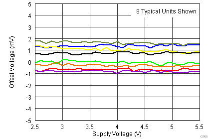
TLV3201-Q1 TLV3202-Q1 Offset vs PS.png
Figure 6. Offset Voltage vs Power Supply
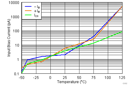
TLV3201-Q1 TLV3202-Q1 Bias Current vs temperature vs supply.png
Figure 8. Input Bias Current and Input Offset Current
vs Temperature
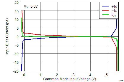
TLV3201-Q1 TLV3202-Q1 IB vs CM 5p5.png
Figure 10. Input Bias Current and Input Offset Current
vs Common-Mode Input Voltage
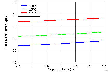
TLV3201-Q1 TLV3202-Q1 IQ vs Supply.png
Figure 12. Quiescent Current vs Supply Voltage
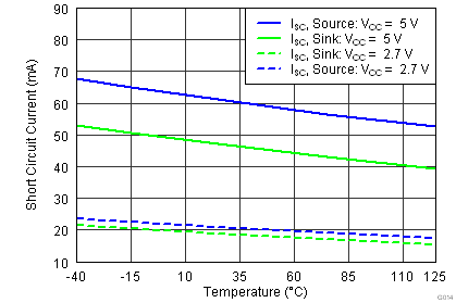
TLV3201-Q1 TLV3202-Q1 Isc vs Temperature.png
Figure 14. Short-Circuit Current vs Temperature
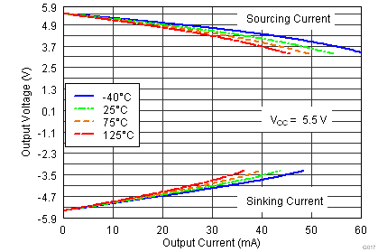
TLV3201-Q1 TLV3202-Q1 IOUT vs Vout 5p5.png
Figure 16. Output Voltage vs Output Current
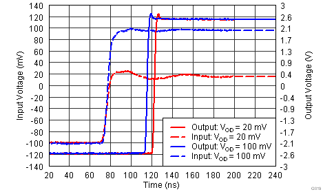
TLV3201-Q1 TLV3202-Q1 Prop Delay LH.png
Figure 18. Propagation Delay Rising Edge
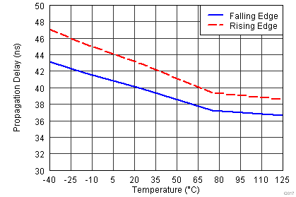
TLV3201-Q1 TLV3202-Q1 Prop vs Temperature.png
Figure 20. Propagation Delay vs Temperature
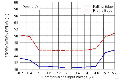
TLV3201-Q1 TLV3202-Q1 Prop vs VCM 5p5.png
Figure 22. Propagation Delay vs Common-Mode Voltage
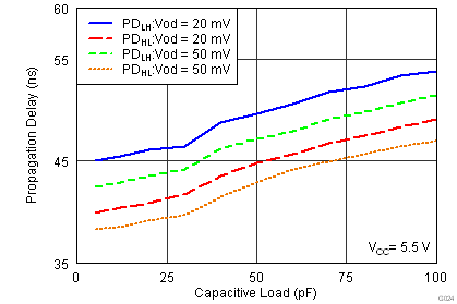
TLV3201-Q1 TLV3202-Q1 cap load_vs_prop_delay.png
Figure 24. Propagation Delay vs Capacitive Load