ZHCSEH4A September 2015 – December 2015 TLV27L2-Q1
PRODUCTION DATA.
7 Specifications
7.1 Absolute Maximum Ratings
over operating free-air temperature range (unless otherwise noted)(1)| MIN | MAX | UNIT | ||
|---|---|---|---|---|
| VS | Supply voltage | 16.5 | V | |
| VI | Input voltage(2) | VS | V | |
| VID | Differential input voltage | VS | V | |
| IO | Output current | 100 | mA | |
| Continuous total power dissipation | See the Thermal Information Table | |||
| TJ | Maximum junction temperature | 150 | °C | |
| TA | Operating free-air temperature | –40 | 125 | °C |
| Lead temperature 1,6 mm (1/16 inch) from case for 10 seconds | 300 | °C | ||
| Tstg | Storage temperature | –65 | 125 | °C |
(1) Stresses beyond those listed under Absolute Maximum Ratings may cause permanent damage to the device. These are stress ratings only, which do not imply functional operation of the device at these or any other conditions beyond those indicated under Recommended Operating Conditions. Exposure to absolute-maximum-rated conditions for extended periods may affect device reliability.
(2) Relative to the V–.
7.2 ESD Ratings
| VALUE | UNIT | ||||
|---|---|---|---|---|---|
| V(ESD) | Electrostatic discharge | Human-body model (HBM), per AEC Q100-002(1) | ±2000 | V | |
| Charged-device model (CDM), per AEC Q100-011 | ±1000 | ||||
(1) AEC Q100-002 indicates that HBM stressing shall be in accordance with the ANSI/ESDA/JEDEC JS-001 specification.
7.3 Recommended Operating Conditions
| MIN | MAX | UNIT | |||
|---|---|---|---|---|---|
| VS | Supply voltage | Dual supply | ±1.35 | ±8 | V |
| Single supply | 2.7 | 16 | |||
| Input common-mode voltage | –0.2 | VS – 1.2 | V | ||
| TA | Operating free-air temperature | –40 | 125 | °C | |
7.4 Thermal Information
| THERMAL METRIC(1) | TLV27L2-Q1 | UNIT | |
|---|---|---|---|
| D (SOIC) | |||
| 8 PINS | |||
| RθJA | Junction-to-ambient thermal resistance | 122.2 | °C/W |
| RθJC(top) | Junction-to-case (top) thermal resistance | 70.5 | °C/W |
| RθJB | Junction-to-board thermal resistance | 62.5 | °C/W |
| ψJT | Junction-to-top characterization parameter | 22.3 | °C/W |
| ψJB | Junction-to-board characterization parameter | 62.0 | °C/W |
| RθJC(bot) | Junction-to-case (bottom) thermal resistance | N/A | °C/W |
(1) For more information about traditional and new thermal metrics, see the Semiconductor and IC Package Thermal Metrics application report, SPRA953.
7.5 Electrical Characteristics
at recommended operating conditions, VS = 2.7 V, 5 V, and 10 V (unless otherwise noted)| PARAMETER | TEST CONDITIONS | TA(1) | MIN | TYP | MAX | UNIT | |||
|---|---|---|---|---|---|---|---|---|---|
| DC PERFORMANCE | |||||||||
| VIO | Input offset voltage | VIC = VS / 2, VO = VS / 2, RL = 100 kΩ, RS = 50 Ω |
25°C | 0.5 | 5 | mV | |||
| Full range | 7 | ||||||||
| αVIO | Offset voltage drift | VIC = VS / 2, VO = VS / 2, RL = 100 kΩ, RS = 50 Ω |
25°C | 1.1 | µV/°C | ||||
| CMRR | Common-mode rejection ratio | VIC = 0 V to VS – 1.2 V, RS = 50 Ω | 25°C | 71 | 86 | dB | |||
| Full range | 70 | ||||||||
| AVD | Large-signal differential voltage amplification | VO(PP) = VS / 2, RL = 100 kΩ, |
VS = 2.7 V, 5 V | 25°C | 80 | 100 | dB | ||
| Full range | 77 | ||||||||
| VS = ±5 V | 25°C | 77 | 82 | ||||||
| Full range | 74 | ||||||||
| INPUT CHARACTERISTICS | |||||||||
| IIO | Input offset current | VIC = VS / 2, VO = VS / 2, RL = 100 kΩ, RS = 50 Ω |
≤ 25°C | 1 | 60 | pA | |||
| ≤ 70°C | 100 | ||||||||
| ≤ 125°C | 1000 | ||||||||
| IIB | Input bias current | VIC = VS / 2, VO = VS / 2, RL = 100 kΩ, RS = 50 Ω |
≤ 25°C | 1 | 60 | pA | |||
| ≤ 70°C | 200 | ||||||||
| ≤ 125°C | 1000 | ||||||||
| ri(d) | Differential input resistance | ≤ 25°C | 1000 | GΩ | |||||
| CIC | Common-mode input capacitance | f = 1 kHz | ≤ 25°C | 8 | pF | ||||
| POWER SUPPLY | |||||||||
| IQ | Quiescent current (per channel) | VO = VS/2 | 25°C | 7 | 11 | µA | |||
| Full range | 16 | ||||||||
| PSRR | Power supply rejection ratio (ΔVS/ΔVIO) |
No load, VS = 2.7 V to 16 V, VIC = VS / 2 V |
25°C | 74 | 82 | dB | |||
| Full range | 70 | ||||||||
| OUTPUT CHARACTERISTICS | |||||||||
| VO | Output voltage swing from rail | VIC = VS / 2, IOL = 100 µA |
VS = 2.7 V | 25°C | 160 | 200 | mV | ||
| Full range | 220 | ||||||||
| VS = 5 V | 25°C | 85 | 120 | ||||||
| Full range | 200 | ||||||||
| VS = ±5 V | 25°C | 50 | 120 | ||||||
| Full range | 150 | ||||||||
| VIC = VS / 2, IOL = 500 µA |
VS = 5 V | 25°C | 420 | 800 | |||||
| Full range | 900 | ||||||||
| VS = ±5 V | 25°C | 200 | 400 | ||||||
| Full range | 500 | ||||||||
| IO | Output current | VO = 0.5 V from rail, VS = 2.7 V | 25°C | 400 | µA | ||||
| DYNAMIC PERFORMANCE | |||||||||
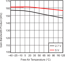
| GBP | Gain bandwidth product | RL = 100 kΩ, CL = 10 pF, f = 1 kHz | 25°C | 160 | kHz | ||||
| SR | Slew rate at unity gain | VO(pp) = 1 V, RL = 100 kΩ, CL = 50 pF |
25°C | 0.06 | V/µs | ||||
| –40°C | 0.05 | ||||||||
| 125°C | 0.8 | ||||||||
| φM | Phase margin | RL = 100 kΩ, CL = 50 pF | 25°C | 62 | ° | ||||
| ts | Settling time (0.1%) | V(STEP)pp = 1 V, AV = –1, rise | 25°C | 62 | µs | ||||
| CL = 50 pF, RL = 100 kΩ, fall | 44 | ||||||||
| NOISE AND DISTORTION PERFORMANCE | |||||||||
| Vn | Equivalent input noise voltage | f = 1 kHz | 25°C | 89 | nV/√Hz | ||||
| In | Equivalent input noise current | f = 1 kHz | 25°C | 0.6 | nV/√Hz | ||||
(1) Full range is –40°C to 125°C for I suffix.
7.6 Typical Characteristics
Table 1. Table of Graphs
| FIGURE | ||
|---|---|---|
| Input offset voltage (VIO) | vs Common-mode input voltage (VIC) | Figure 1, Figure 2, Figure 3 |
| Input bias and offset current (IIB and IIO) | vs Free-air temperature (TA) | Figure 4 |
| High-level output voltage (VOH) | vs High-level output current (IOH) | Figure 5, Figure 7, Figure 9 |
| Low-level output voltage (VOL) | vs Low-level output current (IOL) | Figure 6, Figure 8, Figure 10 |
| Quiescent current (IQ) | vs Supply voltage (VS) | Figure 11 |
| vs Free-air temperature (TA) | Figure 12 | |
| Supply voltage and supply current ramp up | Figure 13 | |
| Differential voltage gain and phase shift (AVD) | vs Frequency (f) | Figure 14 |
| Gain-bandwidth product (GBP) | vs Free-air temperature (TA) | Figure 15 |
| Phase margin (φm) | vs Load capacitance (CL) | Figure 16 |
| Common-mode rejection ratio (CMRR) | vs Frequency (f) | Figure 17 |
| Power supply rejection ratio (PSRR) | vs Frequency (f) | Figure 18 |
| Input referred noise voltage | vs Frequency (f) | Figure 19 |
| Slew rate (SR) | vs Free-air temperature (TA) | Figure 20 |
| Peak-to-peak output voltage (VO(PP)) | vs Frequency (f) | Figure 21 |
| Inverting small-signal response | Figure 22 | |
| Inverting large-signal response | Figure 23 | |
| Crosstalk | vs Frequency (f) | Figure 24 |
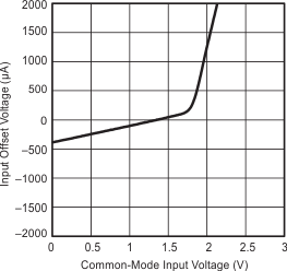
| VS = 2.7 V | TA = 25°C |
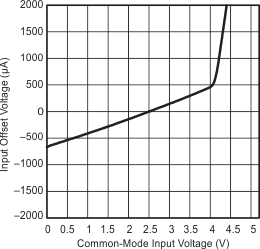
| VS = 5 V | TA = 25°C |
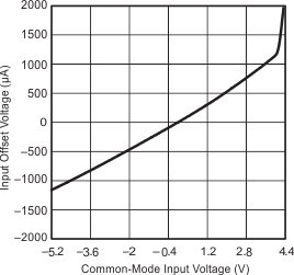
| VS = ±5 VDC | TA = 25°C |
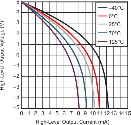
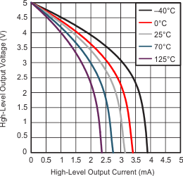
| VS = 5 V |
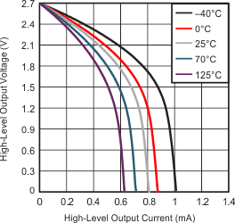
| VS = 2.7 V |
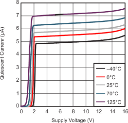
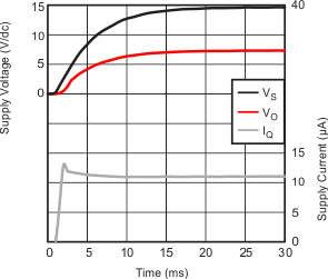
| VS = 0 to 15 V | RL = 100 Ω | CL = 10 pF |
| TA = 25°C |
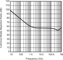
| VS = 5 V | TA = 25°C |
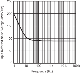
| VS = 5 V | G = 2 | RF = 100 kΩ |
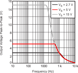
| RL = 100 kΩ | CL = 10 pF | THD+N ≤ 5% |
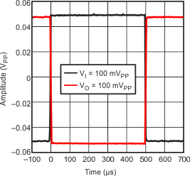
| VS = 5 V | G = –1 | VO = 100 mVPP |
| RL = 100 kΩ | CL = 10 pF | f = 1 kHz |
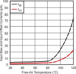
| VS = 5 V | VIC = 2.5 V | VO = 2.5 V |
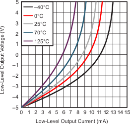
| VS = ±5 V |
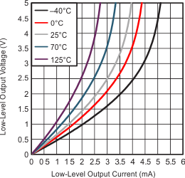
| VS = 5 V |
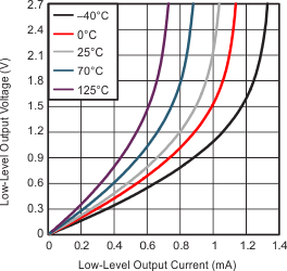
| VS = 2.7 V |
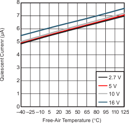
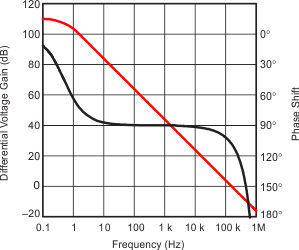
| VS = 5 V | RL = 100 Ω | CL = 10 pF |
| TA = 25°C |
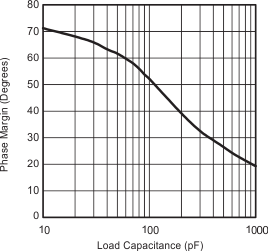
| VS = 5 V | RL = 100 kΩ | TA = 25°C |
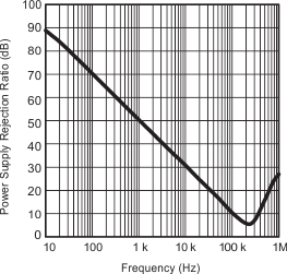
| VS = ±2.5 V | TA = 25°C |
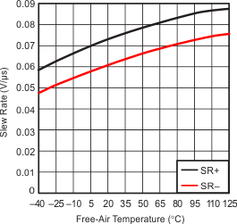
| VS = 5 V | G = 1 | VO = 1 V |
| RL = 100 kΩ | CL = 50 pF |
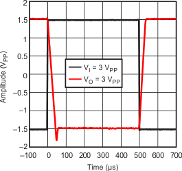
| VS = 5 V | G = –1 | VO = 3 VPP |
| RL = 100 kΩ | CL = 10 pF | f = 1 kHz |
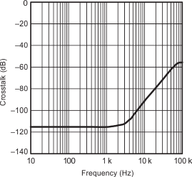
| VS = 5 V | G = –1 | TA = 25°C |
| RL = 2 kΩ | CL = 10 pF | Channel 1 to 2 |