ZHCSEH4A September   2015  – December 2015 TLV27L2-Q1

PRODUCTION DATA.  

  1. 特性
  2. 应用
  3. 说明
  4. 修订历史记录
  5. Selection Guide
  6. Pin Configuration and Functions
  7. Specifications
    1. 7.1 Absolute Maximum Ratings
    2. 7.2 ESD Ratings
    3. 7.3 Recommended Operating Conditions
    4. 7.4 Thermal Information
    5. 7.5 Electrical Characteristics
    6. 7.6 Typical Characteristics
  8. Detailed Description
    1. 8.1 Overview
    2. 8.2 Functional Block Diagram
    3. 8.3 Feature Description
      1. 8.3.1 Offset Voltage
    4. 8.4 Device Functional Modes
  9. Application and Implementation
    1. 9.1 Application Information
      1. 9.1.1 General Configurations
    2. 9.2 Typical Application
      1. 9.2.1 Design Requirements
      2. 9.2.2 Detailed Design Procedure
        1. 9.2.2.1 Shunt Resistor (RSHUNT)
        2. 9.2.2.2 Operational Amplifiers
        3. 9.2.2.3 Reference Voltage Resistors (R5-R6)
        4. 9.2.2.4 Difference Amplifier Gain Setting Resistors (R1-R4)
      3. 9.2.3 Application Curve
  10. 10Power Supply Recommendations
  11. 11Layout
    1. 11.1 Layout Guidelines
    2. 11.2 Layout Example
    3. 11.3 General Power Dissipation Considerations
  12. 12器件和文档支持
    1. 12.1 文档支持
      1. 12.1.1 相关文档
    2. 12.2 社区资源
    3. 12.3 商标
    4. 12.4 静电放电警告
    5. 12.5 Glossary
  13. 13机械、封装和可订购信息

封装选项

机械数据 (封装 | 引脚)
散热焊盘机械数据 (封装 | 引脚)
订购信息

Pin Configuration and Functions

D Package
8-Pin SOIC
Top View
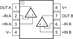
TLV27L2-Q1 po_slos922.gif

Pin Functions

PIN I/O(1) DESCRIPTION
NAME NO.
+IN A 3 I Noninverting input, channel A
+IN B 5 I Noninverting input, channel B
–IN A 2 I Inverting input, channel A
–IN B 6 I Inverting input, channel B
OUT A 1 O Output, channel A
OUT B 7 O Output, channel B
V+ 8 Positive (highest) power supply
V– 4 Negative (lowest) power supply
I = input, O = output