ZHCSAW0C February 2013 – October 2016 TLC59731
PRODUCTION DATA.
- 1 特性
- 2 应用范围
- 3 说明
- 4 修订历史记录
- 5 Pin Configuration and Functions
- 6 Specifications
- 7 Parameter Measurement Information
- 8 Detailed Description
- 9 Application and Implementation
- 10Power Supply Recommendations
- 11Layout
- 12器件和文档支持
- 13机械、封装和可订购信息
8 Detailed Description
8.1 Overview
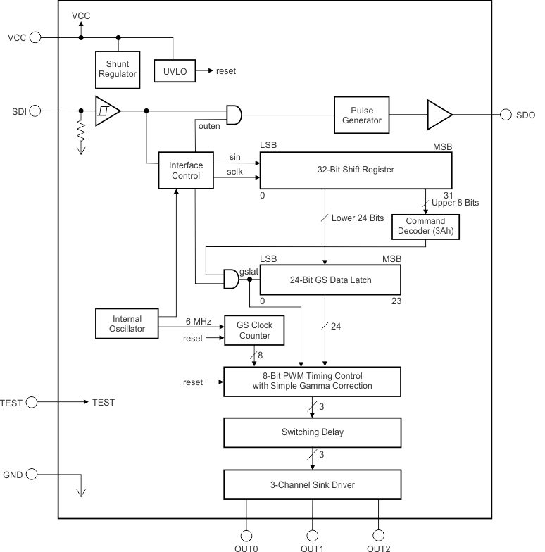
The TLC59731 is a 3-channel constant-current sink driver. Each channel has an individually-adjustable, 256-step, pulse-width modulation (PWM) grayscale (GS) brightness control. GS data are input through a serial single-wire interface port.
The TLC59731 has a 50-mA current capability. The maximum current value of each channel is determined by the external resistor. The TLC59731 can function without external CLK signals because the device is integrated with a 6-MHz internal oscillator.
The TLC59731 is integrated with a shunt regulator that can be used for higher VCC power-supply voltage applications.
8.2 Functional Block Diagram
8.3 Feature Description
8.3.1 Sink Current Value Setting
The typical sink current value of each channel (IOUTn) can be set by resistor (RLn) that is placed between the LED cathode and OUTn pins; see Figure 10. The typical sink current value can be calculated by Equation 1 and the typical resistor value can be calculated by Equation 2.

where
- n = 0 to 2

where
- n = 0 to 2
- VLED = the LED anode voltage
- VF_TOTAL = the total LED forward voltage
- VOUTn = the OUTn output voltage
Note that the typical VOUTn value is 0.6 V with a 40-mA output current, as shown in Figure 4.
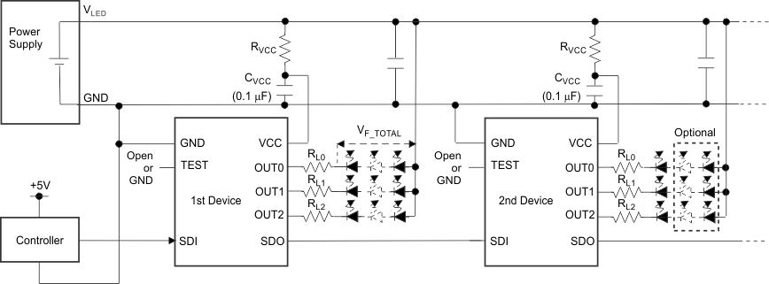 Figure 10. Internal Shunt Regulator Mode Application Circuit
8.3.2 Resistor and Capacitor Value Setting for Shunt Regulator
The TLC59731 internally integrates a shunt regulator to regulate VCC voltage. Figure 4 shows an application circuit that uses the internal shunt regulator through a resistor, RVCC. The recommended RVCC value can be calculated by Equation 3.

Table 1 shows the typical resistor value for several VLED voltages. Note that the CVCC value must be 0.1 μF.
Table 1. Resistor Example for Shunt Resistor Versus LED Voltage
| VLED (V) | RVCC (Ω) | RESISTOR WATTAGE (W) |
|---|---|---|
| 9 | 470 | 0.02 |
| 12 | 910 | 0.04 |
| 18 | 1800 | 0.08 |
| 24 | 2700 | 0.12 |
8.3.3 Grayscale (GS) Control
This control feature is an 8-bit (256-step) grayscale (GS) control that provides a wide range of color generation. Connect the LEDs to the device OUTn pins, as described in the Layout Guidelines section.
8.3.4 EasySet and Shunt Regulator
This device includes a single-wire serial interface (EasySet) and a shunt regulator. The total number of wires for power supply and data write operations can be reduced with the EasySet and shunt regulator included in the design.
8.3.5 No Limit Cascading
This feature results in no limitation on the number of total cascaded devices used in series in an application. This advantage is attained because a timing-adjusted pulse generator is implemented in the device.
8.3.6 Connector Design
When the connector pin of the device application printed circuit board (PCB) is connected or disconnected to other PCBs, the power must be turned off to avoid device malfunction or failure. Furthermore, designing the connector GND pin to be longer than other pins (as shown in Figure 11) is preferable. This arrangement allows the GND line to either be connected first or disconnected last, which is imperative for proper device function.
 Figure 11. Connector Pin Design Application
8.4 Device Functional Modes
8.4.1 Grayscale (GS) Function (PWM Control)
The TLC59731 can adjust the brightness of each output channel using a pulse width modulation (PWM) control scheme. The PWM data bit length for each output is 8 bits. The architecture of 8 bits per channel results in 256 brightness steps, from 0% to 99.98% ON-time duty cycle.
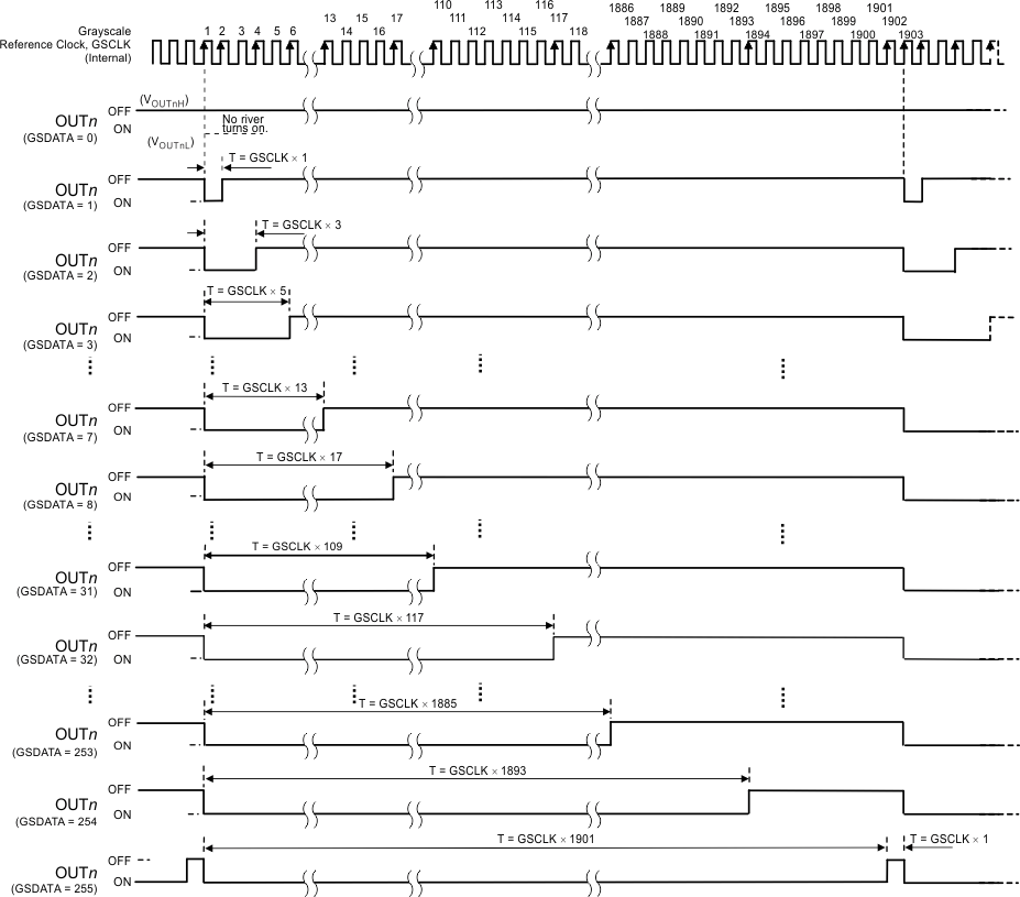
The PWM operation for OUTn is controlled by an 8-bit grayscale (GS) counter. The GS counter increments on each internal GS clock (GSCLK) rising edge. All OUTn are turned on when the GS count is ‘1’, except when OUTn are programed to GS data '0' in the 24-bit GS data latch. After turning on, each output turns off when the GS counter value exceeds the programmed GS data for the output. The GS counter resets to 00h and all outputs are forced off when the GS data are written to the 24-bit GS data latch. Afterwards, the GS counter begins incrementing and PWM control is started from the next internal GS clock.
Table 2 summarizes the GS data values versus the output ideal ON-time duty cycle. The on-time duty cycle is not proportional to the GS data because a simple gamma correction is implemented in the TLC59731. Furthermore, actual ON-time differs from the ideal ON-time because the output drivers and control circuit have some timing delay. When the device is powered on, all outputs are forced off and remain off until the non-zero GS data are written to the 24-bit GS data latch.
Table 2. Output Duty Cycle and Total ON-Time vs GS Data
| GS DATA | NO. OF GSCLKs OUTn TURNS ON | NO. OF GSCLKs OUTn TURNS OFF | TOTAL IDEAL TIME (µs) | ON-TIME DUTY (%) | |
|---|---|---|---|---|---|
| DECIMAL | HEX | ||||
| 0 | 0 | Off | Off | 0 | 0 |
| 1 | 1 | 1 | 2 | 0.08 | 0.02 |
| 2 | 2 | 1 | 4 | 0.17 | 0.05 |
| 3 | 3 | 1 | 6 | 0.8 | 0.3 |
| — | — | — | — | — | — |
| 6 | 6 | 1 | 12 | 1.8 | 0.6 |
| 7 | 7 | 1 | 14 | 2.2 | 0.7 |
| 8 | 8 | 1 | 18 | 2.8 | 0.9 |
| 9 | 9 | 1 | 22 | 3.5 | 1.1 |
| 10 | 10 | 1 | 26 | 4.2 | 1.3 |
| — | — | — | — | — | — |
| 30 | 1E | 1 | 106 | 17.5 | 5.5 |
| 31 | 1F | 1 | 110 | 18.2 | 5.7 |
| 32 | 20 | 1 | 118 | 19.5 | 6.2 |
| 33 | 21 | 1 | 126 | 20.8 | 6.6 |
| 34 | 22 | 1 | 134 | 22.2 | 7.0 |
| — | — | — | — | — | — |
| 62 | 3E | 1 | 358 | 59.5 | 18.8 |
| 63 | 3F | 1 | 366 | 60.8 | 19.2 |
| 64 | 40 | 1 | 374 | 62.2 | 19.6 |
| 65 | 41 | 1 | 382 | 63.5 | 20.0 |
| 66 | 42 | 1 | 390 | 64.8 | 20.5 |
| — | — | — | — | — | — |
| 127 | 7F | 1 | 878 | 146.2 | 46.1 |
| 128 | 80 | 1 | 886 | 147.5 | 46.5 |
| 129 | 81 | 1 | 894 | 148.8 | 47.0 |
| — | — | — | — | — | — |
| 253 | FD | 1 | 1886 | 314.2 | 99.1 |
| 254 | FE | 1 | 1894 | 315.5 | 99.5 |
| 255 | FF | 1 | 1902 | 316.8 | 99.9 |
8.4.1.1 PWM Control
The GS counter keeps track of the number of grayscale reference clocks (GSCLKs) from the internal oscillator. Each output stays on when the counter is less than or equal to the programmed GS value. Each output turns off when the GS counter is greater than the GS value in the 24-bit GS data latch. Figure 12 shows the PWM operation timing.
8.5 Programming
8.5.1 One-Wire Interface (EasySet) Data Writing Method
There are four sequences to write GS data into the TLC59731 through a single-wire interface. This section discusses each sequence in detail.
8.5.1.1 Data Transfer Rate (TCYCLE) Measurement Sequence
The TLC59731 measures the time between the first and second SDI rising edges either after the device is powered up or when the GS data latch sequence is executed (as described in the GS Data Latch Sequence (GSLAT) section) and the time is internally stored as tCYCLE. tCYCLE serves as a base time used to recognize one complete data write operation, a 32-bit data write operation, and a GS data write operation to the GS data latch. tCYCLE can be set between 1.66 µs and 50 µs (fCLK(SDI) = 20 kHz to 600 kHz). In this sequence, two instances of data 0 are written to the LSB side of the 32-bit shift register. Figure 13 shows the tCYCLE measurement timing.
 Figure 13. Data Transfer Rate (TCYCLE) Measurement
8.5.1.2 Data 0 and Data 1 Write Sequence (Data Write Sequence)
When the second SDI rising edge is not input before 50% of tCYCLE elapses from the first SDI rising edge input, the second rising edge is recognized as data 0. When the second SDI rising edge is input before 50% of tCYCLE elapses from the first SDI rising edge input, the second rising edge is recognized as data 1. This write sequence must be repeated 30 times after the tCYCLE measurement sequence to send the write command to the lower 6-bit (3Ah) and 24-bit GS data. Figure 14 shows the data 0 and 1 write timing.
 Figure 14. Data 0 and 1 Write Operation
8.5.1.3 One Communication Cycle End of Sequence (EOS)
One communication cycle end of sequence (EOS) must be input after the 32-bit data are written because the TLC59731 does not count the number of input data. When SDI is held low for the EOS hold time (tH0), the 32-bit shift register values are locked and a buffered SDI signal is output from SDO to transfer GS data to the next device. Figure 15 shows the EOS timing.
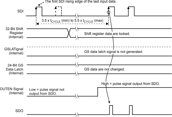 Figure 15. End of Sequence (EOS)
8.5.1.4 GS Data Latch (GSLAT) Sequence
A GS data latch (GSLAT) sequence must be input after the 32-bit data for all cascaded devices are written. When SDI is held low for the data latch hold time (tH1), the 32-bit shift register data in all devices are copied to the GS data latch in each device. Furthermore, PWM control starts with the new GS data at the same time. Figure 16 shows the GSLAT timing.
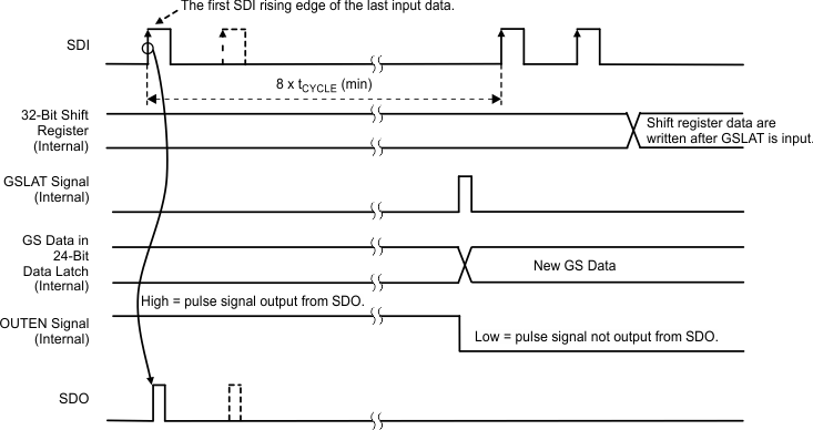 Figure 16. GS Data Latch Sequence (GSLAT)
8.5.1.5 How to Control Devices Connected in Series
The 8-bit write command and 24-bit grayscale (GS) data for OUT0 to OUT2 (for a total of 32 bits of data) must be written to the device. Figure 17 shows the 32-bit data packet configuration. When multiple devices are cascaded (see Figure 18), N times the packet must be written into each TLC59731 in order to control all devices. There is no limit on how many devices can be cascaded, as long as proper VCC voltage is supplied. The packet for all devices must be written again whenever any GS data changes.
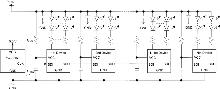 Figure 18. Cascade Connection of N TLC59731 Units (Internal Shunt Regulator Mode)
Figure 19 shows the 32-bit data packet, EOS, and GSLAT input timing of all devices. The function setting write procedure and display control is as follows:
- Power up VCC (VLED); all OUTn are off because GS data are not written yet.
- Write the 32-bit data packet (MSB-first) for the first device using tCYCLE and the data write sequences illustrated in and . The first 8-bits of the 32-bit data packet are used as the write command. The write command must be 3Ah (00111010b); otherwise, the 24-bit GS data in the 32-bit shift register are not copied to the 24-bit GS data latch.
- Execute one communication cycle EOS (refer to ) for the first device.
- Write the 32-bit data packet for the second TLC59731 as described step 2. However, tCYCLE must be set to the same timing as the first device.
- Execute one communication cycle EOS for the second device.
- Repeat Steps 4 and 5 until all devices have GS data.
- The number of total bits is 32 × N. After all data are written, execute a GSLAT sequence as described in in order to copy the 24-bit LSBs in the 32-bit shift resister to the 24-bit GS data latch in each device; PWM control starts with the written GS data at the same time.
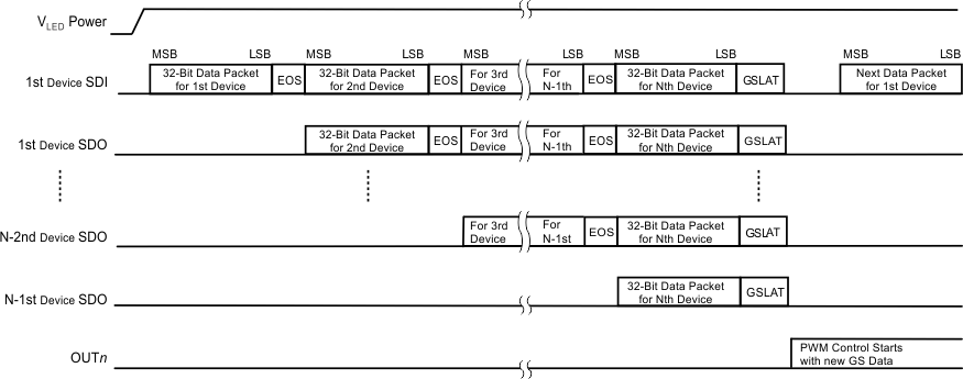 Figure 19. Data Packet Input Order for N TLC59731 Units
8.6 Register Maps
8.6.1 Register and Data Latch Configuration
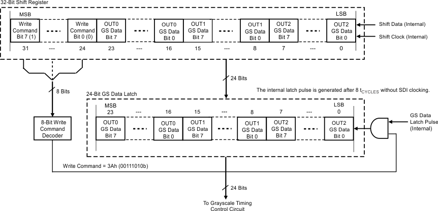
The TLC59731 has a 32-bit shift register and a 24-bit data latch that stores GS data. When the internal GS data latch pulse is generated and the data of the eight MSBs in the shift register are 3Ah, the lower 24-bit data in the 32-bit shift register are copied into the 24-bit GS data latch. If the data of the eight MSBs is not 3Ah, the 24-bit data are not copied into the 24-bit GS data latch. Figure 20 shows the shift register and GS data latch configurations. Table 3 shows the 32-bit shift register bit assignment.
Table 3. 32-Bit Shift Register Data Bit Assignment
| BIT | BIT NAME | CONTROLLED CHANNEL AND FUNCTIONS |
|---|---|---|
| 0 to 7 | GSOUT2 | GS data bits 0 to 7 for OUT2 |
| 8 to 15 | GSOUT1 | GS data bits 0 to 7 for OUT1 |
| 16 to 23 | GSOUT0 | GS data bits 0 to 7 for OUT0 |
| 24 to 32 | WRTCMD | Data write command (3Ah) for GS data. The lower 24-bit GS data in the 32-bit shift register are copied to the GS data latch when the internal GS latch is generated (when these data bits are 3Ah, 00111010b). |
