ZHCSAX3B March 2013 – May 2014 TLC5973
PRODUCTION DATA.
- 1 特性
- 2 应用范围
- 3 说明
- 4 修订历史记录
- 5 Pin Configuration and Functions
- 6 Specifications
- 7 Parameter Measurement Information
- 8 Detailed Description
- 9 Applications and Implementation
- 10Power Supply Recommendations
- 11Layout
- 12器件和文档支持
- 13机械封装和可订购信息
5 Pin Configuration and Functions
D Package
SO-8
(Top View)
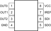
Pin Functions
| PIN | I/O | DESCRIPTION | |
|---|---|---|---|
| NAME | NO. | ||
| OUT0 | 1 | O | Constant sink current driver outputs. Multiple outputs can be configured in parallel to increase the sink drive current capability. Different voltages can be applied to each output. |
| OUT1 | 2 | O | |
| OUT2 | 3 | O | |
| GND | 4 | — | Power ground |
| SDO | 5 | O | Serial data output |
| SDI | 6 | I | Serial data input. This pin is internally pulled down to GND with a 1-MΩ (typ) resistor. |
| IREF | 7 | I/O | Output current programming pin. A resistor connected between IREF and GND sets the current for each constant-current output. Place the external resistor close to the device. |
| VCC | 8 | — | Power-supply voltage |