ZHCSAX3B March   2013  – May 2014 TLC5973

PRODUCTION DATA.  

  1. 特性
  2. 应用范围
  3. 说明
  4. 修订历史记录
  5. Pin Configuration and Functions
  6. Specifications
    1. 6.1 Absolute Maximum Ratings
    2. 6.2 Handling Ratings
    3. 6.3 Recommended Operating Conditions
    4. 6.4 Thermal Information
    5. 6.5 Electrical Characteristics
    6. 6.6 Switching Characteristics
    7. 6.7 Typical Characteristics
  7. Parameter Measurement Information
    1. 7.1 Pin-Equivalent Input and Output Schematic Diagrams
    2. 7.2 Test Circuits
    3. 7.3 Timing Diagrams
  8. Detailed Description
    1. 8.1 Overview
    2. 8.2 Functional Block Diagram
    3. 8.3 Feature Description
      1. 8.3.1 Grayscale (GS) Control
      2. 8.3.2 EasySet and Shunt Regulator
      3. 8.3.3 No Limit Cascading
      4. 8.3.4 Constant Sink Current Value
      5. 8.3.5 Connector Design
    4. 8.4 Device Functional Modes
      1. 8.4.1 Grayscale (GS) Function (PWM Control)
        1. 8.4.1.1 PWM Control
      2. 8.4.2 One-Wire Interface (EasySet) Data Writing Method
        1. 8.4.2.1 Data Transfer Rate (tCYCLE) Measurement Sequence
        2. 8.4.2.2 Data ‘0’ and Data ‘1’ Write Sequence (Data Write Sequence)
        3. 8.4.2.3 One Communication Cycle End of Sequence (EOS)
        4. 8.4.2.4 GS Data Latch (GSLAT) Sequence
    5. 8.5 Programming
      1. 8.5.1 Controlling Devices Connected in Series
    6. 8.6 Register Maps
      1. 8.6.1 Register and Data Latch Configuration
  9. Applications and Implementation
    1. 9.1 Application Information
    2. 9.2 Typical Applications
      1. 9.2.1 No Internal Shunt Regulator Mode 1
        1. 9.2.1.1 Design Requirements
        2. 9.2.1.2 Detailed Design Procedure
        3. 9.2.1.3 Application Curve
      2. 9.2.2 No Internal Shunt Regulator Mode 2
        1. 9.2.2.1 Design Requirements
        2. 9.2.2.2 Detailed Design Procedure
        3. 9.2.2.3 Application Curve
      3. 9.2.3 Internal Shunt Regulator Mode
        1. 9.2.3.1 Design Requirements
        2. 9.2.3.2 Detailed Design Procedure
        3. 9.2.3.3 Application Curves
  10. 10Power Supply Recommendations
  11. 11Layout
    1. 11.1 Layout Guidelines
    2. 11.2 Layout Example
  12. 12器件和文档支持
    1. 12.1 Trademarks
    2. 12.2 Electrostatic Discharge Caution
    3. 12.3 Glossary
  13. 13机械封装和可订购信息

封装选项

机械数据 (封装 | 引脚)
散热焊盘机械数据 (封装 | 引脚)
订购信息

11 Layout

11.1 Layout Guidelines

  • The resistor used for the output current setting should be placed near the IREF and GND pins of the device.
  • The decoupling capacitor and the shunt regulator resistor should be placed near the VCC pin of the device.

11.2 Layout Example

ai_layout_bvs225.gif
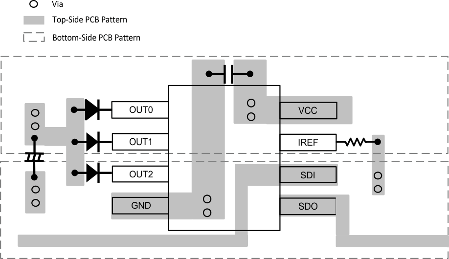
Figure 30. Layout Example