ZHCSCX6 October 2014 TLC5957
PRODUCTION DATA.
- 1 特性
- 2 应用范围
- 3 说明
- 4 典型应用电路(多个菊花链 TLC5957)
- 5 修订历史记录
- 6 Pin Configuration and Functions
- 7 Specifications
- 8 Parameter Measurement Information
-
9 Detailed Description
- 9.1 Overview
- 9.2 Functional Block Diagram
- 9.3
Device Functional Modes
- 9.3.1 Brightness Control (BC) Function
- 9.3.2 Color Control (CC) Function
- 9.3.3 Select RIREF For a Given BC
- 9.3.4 Choosing BC/CC For a Different Application
- 9.3.5 LED Open Detection (LOD)
- 9.3.6 Poker Mode
- 9.3.7 Internal Circuit for Caterpillar Removal
- 9.3.8 Internal Pre-charge FET for Ghost Removal
- 9.3.9 Thermal Shutdown (TSD)
- 9.3.10 IREF Resistor Short Protection (ISP)
- 9.3.11 Noise Reduction
- 10Application and Implementation
- 11Power Supply Recommendations
- 12Layout
- 13器件和文档支持
- 14机械封装和可订购信息
12 Layout
12.1 Layout Guidelines
- Place the decoupling capacitor near the VCC pin and GND plane.
- Place the current programming resistor Riref close to IREF pin and IREFGND pin.
- Route the GND pattern as widely as possible for large GND currents. Maximum GND current is approximately 1.2A
- Routing between the LED cathode side and the device OUTXn pin should be as short and straight as possible to reduce wire inductance.
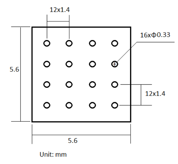
- The PowerPAD™ must be connected to GND plane because the pad is used as power ground pin internally, there will be large current flow through this pad when all channels turn on. Furthermore, this pad should be connected to a heat sink layer by thermal via to reduce device temperature. One suggested thermal via pattern is shown as below. For more information about suggested thermal via pattern and via size, see " PowerPAD Thermally Enhanced Package", SLMA002G.
12.2 Layout Example