SLDS165A December 2008 – December 2014 TLC5941-Q1
PRODUCTION DATA.
- 1 Features
- 2 Applications
- 3 Description
- 4 Revision History
- 5 Pin Configuration and Functions
- 6 Specifications
- 7 Parameter Measurement Information
- 8 Detailed Description
- 9 Application and Implementation
- 10Power Supply Recommendations
- 11Layout
- 12Device and Documentation Support
- 13Mechanical, Packaging, and Orderable Information
9 Application and Implementation
NOTE
Information in the following applications sections is not part of the TI component specification, and TI does not warrant its accuracy or completeness. TI’s customers are responsible for determining suitability of components for their purposes. Customers should validate and test their design implementation to confirm system functionality.
9.1 Application Information
The TLC5941-Q1 device can be used for LED lighting, such as signboards and automotive dashboard back-lighting.
9.2 Typical Application
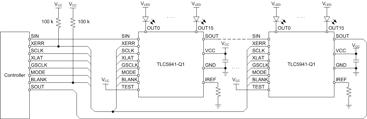 Figure 18. Cascading Devices
9.2.1 Design Requirements
For the design example, use the following as the input parameter.
- VCC = 5 V
- VLED = 5 V – 16 V
- IMAX = 30 mA
9.2.2 Detailed Design Procedure
9.2.2.1 Setting Maximum Channel Current
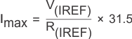
The maximum output current per channel is programmed by a single resistor, R(IREF), which is placed between the IREF pin and the GND pin. The voltage on the IREF pin is set by an internal band gap V(IREF) with a typical value of 1.24 V. The maximum channel current is equivalent to the current flowing through R(IREF) multiplied by a factor of 31.5. The maximum output current can be calculated by Equation 7.
where
- V(IREF) = 1.24 V
- R(IREF) = User-selected external resistor.
The value of Imax must be set between 5 mA and 60 mA. The output current may be unstable if Imax is set lower than 5 mA. Output currents lower than 5 mA can be achieved by setting Imax to 5 mA or higher and then using dot correction.
Figure 1 shows the maximum output current IO versus R(IREF). R(IREF) is the value of the resistor between IREF terminal to GND, and IO is the constant output current of OUT0 to OUT15. A variable power supply may be connected to the IREF pin through a resistor to change the maximum output current per channel. The maximum output current per channel is 31.5 times the current flowing out of the IREF pin.
9.2.2.2 Power Dissipation Calculation
The device power dissipation must be below the power dissipation rate of the device package to ensure correct operation. Equation 8 calculates the power dissipation of device.

where
- VCC: device supply voltage
- ICC: device supply current
- VOUT: TLC5941-Q1 OUTn voltage when driving LED current
- IMAX: LED current adjusted by R(IREF) resistor
- DCn: maximum dot correction value for OUTn
- N: number of OUTn driving LED at the same time
- dPWM: duty cycle defined by BLANK pin or GS PWM value
9.2.2.3 Setting Dot Correction
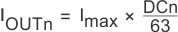
The TLC5941-Q1 device has the capability to fine-adjust the output current of each channel (OUT0 to OUT15) independently which is also called dot correction. This feature is used to adjust the brightness deviations of LEDs connected to the output channels OUT0 to OUT15. Each of the 16 channels can be programmed with a 6-bit word. The channel output can be adjusted in 64 steps from 0% to 100% of the maximum output current Imax. The TEST pin must be connected to VCC to ensure proper operation of the dot correction circuitry. Equation 9 calculates the output current for each output n.
where
- Imax = the maximum programmable output current for each output.
- DCn = the programmed dot correction value for output n (DCn = 0 to 63)
- n = 0 to 15
Figure 19 shows the dot correction data packet format which consists of 6 bits x 16 channel, total 96 bits. The format is Big-Endian format. This means that the MSB is transmitted first, followed by the MSB-1 and so on. The DC 15.5 in Figure 19 stands for the 5th-most significant bit for output 15.
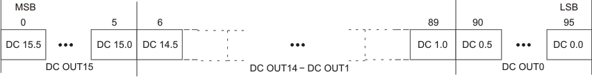 Figure 19. Dot Correction Data Packet Format
When the MODE pin is set to VCC, the TLC5941-Q1 device enters the dot correction data input mode. The length of input shift register becomes 96bits. After all serial data are shifted in, the TLC5941-Q1 device writes the data in the input shift register to DC register when the XLAT pin is high, and holds the data in the DC register when the XLAT pin is low. The DC register is a level triggered latch of the XLAT signal. Because the XLAT pin is a level-triggered signal, SCLK and SIN must not be changed while the XLAT pin is high. After the XLAT pin goes low, data in the DC register is latched and does not change. The BLANK signal does not need to be high to latch in new data. When the XLAT pin goes high, the new dot-correction data immediately becomes valid and changes the output currents if the BLANK pin is low. the XLAT pin has setup time (tsu1) and hold time (th1) to SCLK as shown in Figure 12.
To input data into the dot correction register, the MODE pin must be set to VCC. The internal input shift register is then set to 96-bit width. After all serial data are clocked in, a rising edge of the XLAT pin is used to latch the data into the dot correction register. Figure 20 shows the DC-data input-timing chart.
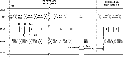 Figure 20. Dot-Correction Data Input-Timing Chart
9.2.2.4 Setting Grayscale
The TLC5941-Q1 device can adjust the brightness of each channel, OUTn, using a PWM control scheme. The use of 12 bits per channel results in 4096 different brightness steps, from 0% to 100% brightness. Equation 10 calculates the brightness level for each output n.

where
- GSn = the programmed grayscale value for output n (GSn = 0 to 4095)
- n = 0 to 15
- Grayscale data for all OUTn
The input shift register enters grayscale data into the grayscale register for all channels simultaneously. The complete grayscale data format consists of 16 × 12 bit words, which forms a 192-bit wide data packet (see Figure 21). The data packet must be clocked in with the MSB first.
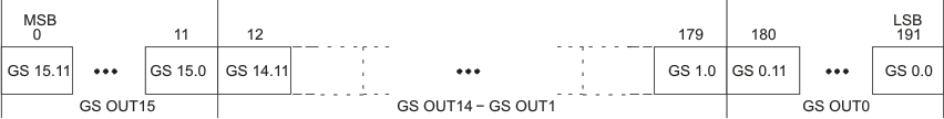 Figure 21. Grayscale Data Packet Format
When the MODE pin is set to GND, the TLC5941-Q1 device enters the grayscale data input mode. The device switches the input shift register to 192-bit width. After all data is clocked in, a rising edge of the XLAT signal latches the data into the grayscale register (see Figure 22). New grayscale data immediately becomes valid at the rising edge of the XLAT signal; therefore, new grayscale data should be latched at the end of a grayscale cycle when BLANK is high. The first GS data input cycle after dot correction requires an additional SCLK pulse after the XLAT signal to complete the grayscale update cycle. All GS data in the input shift register is replaced with status information data (SID) after updating the grayscale register.
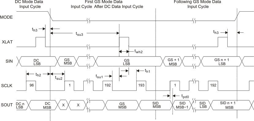 Figure 22. Grayscale Data Input Timing Chart
9.2.2.5 Serial Data Transfer Rate
Figure 18 shows a cascading connection of n TLC5941-Q1 devices connected to a controller, building a basic module of an LED display system. The TLC5941-Q1 device has no limit to the maximum number of ICs that can be cascaded. The maximum number of cascading TLC5941-Q1 devices depends on the application system and is in the range of 40 devices. Equation 11 calculates the minimum frequency needed:
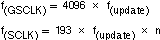
where
- f(GSCLK): minimum frequency needed for GSCLK
- f(SCLK): minimum frequency needed for SCLK and SIN
- f(update): update rate of whole cascading system
- n: number cascaded of TLC5941-Q1 device
9.2.3 Application Curves
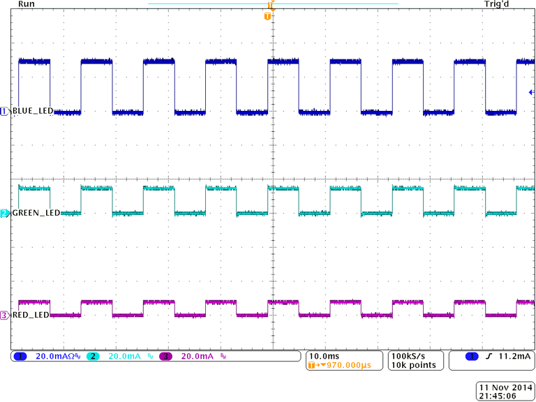
| CH1 DC=63 | CH2 DC=31 | CH3 DC=15 |
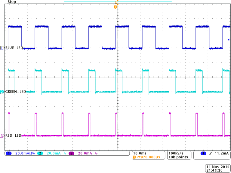
| CH1 GS=512 | CH2 GS=256 | CH3 GS=64 |