ZHCSGH6 June   2017 TLC2274AM-MIL

PRODUCTION DATA.  

  1. 特性
  2. 应用
  3. 说明
  4. 修订历史记录
  5. Pin Configuration and Functions
  6. Specifications
    1. 6.1 Absolute Maximum Ratings
    2. 6.2 ESD Ratings
    3. 6.3 Recommended Operating Conditions
    4. 6.4 Thermal Information
    5. 6.5 Electrical Characteristics VDD = 5 V
    6. 6.6 Electrical Characteristics VDD± = ±5 V
    7. 6.7 Typical Characteristics
  7. Detailed Description
    1. 7.1 Overview
    2. 7.2 Functional Block Diagram
    3. 7.3 Feature Description
    4. 7.4 Device Functional Modes
  8. Application and Implementation
    1. 8.1 Application Information
      1. 8.1.1 Macromodel Information
    2. 8.2 Typical Application
      1. 8.2.1 High-Side Current Monitor
        1. 8.2.1.1 Design Requirements
        2. 8.2.1.2 Detailed Design Procedure
          1. 8.2.1.2.1 Differential Amplifier Equations
        3. 8.2.1.3 Application Curves
  9. Power Supply Recommendations
  10. 10Layout
    1. 10.1 Layout Guidelines
    2. 10.2 Layout Example
  11. 11器件和文档支持
    1. 11.1 接收文档更新通知
    2. 11.2 社区资源
    3. 11.3 商标
    4. 11.4 静电放电警告
    5. 11.5 Glossary
  12. 12机械、封装和可订购信息

封装选项

机械数据 (封装 | 引脚)
散热焊盘机械数据 (封装 | 引脚)
订购信息

Layout

Layout Guidelines

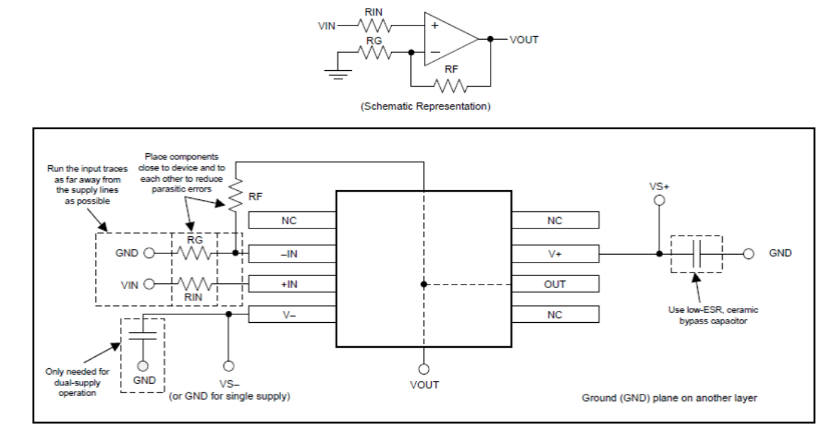
The TLC2274AM-MIL device is a wideband amplifier. To realize the full operational performance of the device, good high-frequency printed-circuit-board (PCB) layout practices are required. Low-loss 0.1-μF bypass capacitors must be connected between each supply pin and ground as close to the device as possible. The bypass capacitor traces should be designed for minimum inductance.

Layout Example

TLC2274AM-MIL Layout Example.gif Figure 57. Layout Example