ZHCSD78 January 2015 TLC2274-HT
PRODUCTION DATA.
- 1 特性
- 2 应用
- 3 说明
- 4 修订历史记录
- 5 Pin Configuration and Functions
-
6 Specifications
- 6.1 Absolute Maximum Ratings
- 6.2 ESD Ratings
- 6.3 Recommended Operating Conditions
- 6.4 Thermal Information
- 6.5 Electrical Characteristics, VDD = 5 V
- 6.6 Operating Characteristics, VDD = 5 V
- 6.7 Electrical Characteristics, VDD± = ±5 V
- 6.8 Operating Characteristics, VDD± = ±5 V
- 6.9 Typical Characteristics
- 7 Detailed Description
- 8 Application and Implementation
- 9 Power Supply Recommendations
- 10Layout
- 11器件和文档支持
- 12机械封装和可订购信息
6 Specifications
6.1 Absolute Maximum Ratings(1)
over operating free-air temperature range (unless otherwise noted)| MIN | MAX | UNIT | |||
|---|---|---|---|---|---|
| VDD+ | Supply voltage(2) | 8 | V | ||
| VDD– | Supply voltage(2) | –8 | V | ||
| VID | Differential input voltage(3) | –16 | 16 | V | |
| VI | Input voltage(2) | Any input | VDD– – 0.3 | VDD+ | V |
| II | Input current | Any input | –5 | 5 | mA |
| IO | Output current | –50 | 50 | mA | |
| Total current into VDD+ | –50 | 50 | mA | ||
| Total current out of VDD− | –50 | 50 | mA | ||
| Duration of short-circuit current at (or below) 25°C(4) | Unlimited | ||||
| TA | Operating free-air temperature | –40 | 150 | °C | |
| Lead temperature 1.6 mm (1/16 inch) from case for 10 s | 260 | °C | |||
| Tstg | Storage temperature | –65 | 150 | °C | |
(1) Stresses beyond those listed under “absolute maximum ratings” may cause permanent damage to the device. These are stress ratings only, and functional operation of the device at these or any other conditions beyond those indicated under “recommended operating conditions” is not implied. Exposure to absolute-maximum-rated conditions for extended periods may affect device reliability.
(2) All voltage values, except differential voltages, are with respect to the midpoint between VDD+ and VDD–.
(3) Differential voltages are at IN+ with respect to IN–. Excessive current will flow if input is brought below VDD– – 0.3 V.
(4) The output may be shorted to either supply. Temperature and/or supply voltages must be limited to ensure that the maximum dissipation rating is not exceeded.
6.2 ESD Ratings
| VALUE | UNIT | ||||
|---|---|---|---|---|---|
| V(ESD) | Electrostatic discharge | Human-body model (HBM), per AEC Q100-002(1) | ±2500 | V | |
| Charged-device model (CDM), per AEC Q100-011 | All pins | ±1500 | |||
(1) AEC Q100-002 indicates that HBM stressing shall be in accordance with the ANSI/ESDA/JEDEC JS-001 specification.
6.3 Recommended Operating Conditions
over operating free-air temperature range (unless otherwise noted)| MIN | MAX | UNIT | ||
|---|---|---|---|---|
| VDD± | Supply voltage | ±2.2 | ±8 | V |
| VI | Input voltage | VDD− | VDD+ −1.5 | V |
| VIC | Common-mode input voltage | VDD− | VDD+ −1.5 | V |
| TA | Operating free-air temperature | −40 | 150 | °C |
6.4 Thermal Information
| THERMAL METRIC(1) | TLC2274 | UNIT | |
|---|---|---|---|
| PW | |||
| 14 PINS | |||
| RθJA | Junction-to-ambient thermal resistance | 106.0 | °C/W |
| RθJC(top) | Junction-to-case (top) thermal resistance | 35.5 | |
| RθJB | Junction-to-board thermal resistance | 47.6 | |
| ψJT | Junction-to-top characterization parameter | 2.4 | |
| ψJB | Junction-to-board characterization parameter | 47.1 | |
(1) For more information about traditional and new thermal metrics, see the IC Package Thermal Metrics application report, SPRA953.
6.5 Electrical Characteristics, VDD = 5 V
at specified free-air temperature, VDD = 5 V (unless otherwise noted)| PARAMETER | TEST CONDITIONS | TA(1) | MIN | TYP | MAX | UNIT | ||
|---|---|---|---|---|---|---|---|---|
| VIO | Input offset voltage | VIC = 0 V, VO = 0 V, |
VDD± = ±2.5 V, RS = 50 Ω |
25°C | 300 | 2500 | μV | |
| Full range | 3000 | |||||||
| αVIO | Temperature coefficient of input offset voltage | 25°C to 125°C | 2 | μV/°C | ||||
| Input offset voltage long-term drift(2) | 25°C | 0.002 | μV/mo | |||||
| IIO | Input offset current | 25°C | 0.5 | 60 | pA | |||
| Full range | 7000 | |||||||
| IIB | Input bias current | 25°C | 1 | pA | ||||
| Full range | ||||||||
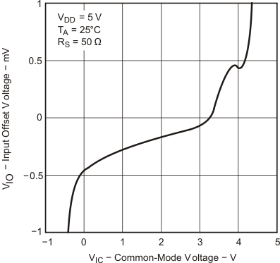
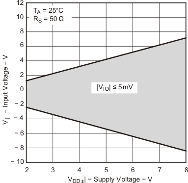
| VICR | Common-mode input voltage range | RS = 50 Ω | |VIO| ≤ 5 mV | 25°C | 0 to 4 | −0.3 to 4.2 | V | |
| Full range | 0 to 3.5 | |||||||
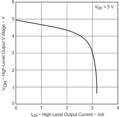
| VOH | High-level output voltage | IOH = −20 μA | 25°C | 4.99 | V | |||
| IOH = −200 μA | 25°C | 4.85 | 4.93 | |||||
| Full range | 4.84 | |||||||
| IOH = −1 mA | 25°C | 4.25 | 4.65 | |||||
| Full range | 4.20 | |||||||
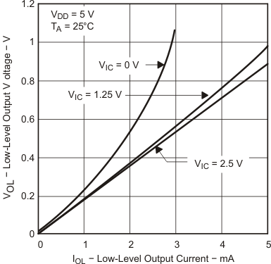
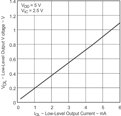
| VOL | Low-level output voltage | VIC = 2.5 V, | IOL = 50 μA | 25°C | 0.01 | V | ||
| VIC = 2.5 V, | IOL = 500 μA | 25°C | 0.09 | 0.15 | ||||
| Full range | 0.16 | |||||||
| VIC = 2.5 V, | IOL = 5 mA | 25°C | 0.9 | 1.5 | ||||
| Full range | 1.6 | |||||||
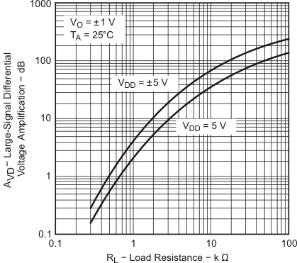
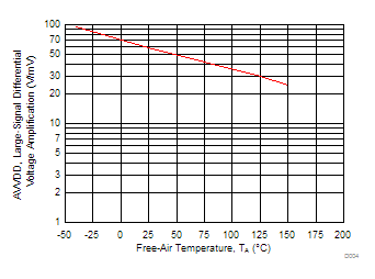
| AVD | Large-signal differential voltage amplification | VIC = 2.5 V, VO = 1 V to 4 V, |
RL = 10 kΩ(3) | 25°C | 10 | 35 | V/mV | |
| Full range | 8 | |||||||
| RL = 1 MΩ(3) | 25°C | 175 | ||||||
| rid | Differential input resistance | 25°C | 1012 | Ω | ||||
| ri | Common-mode input resistance | 25°C | 1012 | Ω | ||||
| ci | Common-mode input capacitance | f = 10 kHz, | N package | 25°C | 8 | pF | ||
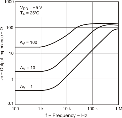
| zo | Closed-loop output impedance | f = 1 MHz, | AV = 10 | 25°C | 140 | Ω | ||
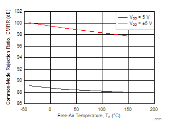
| CMRR | Common-mode rejection ratio | VIC = 0 V to 2.7 V, VO = 2.5 V, |
RS = 50 Ω | 25°C | 70 | 75 | dB | |
| Full range | 69 | |||||||
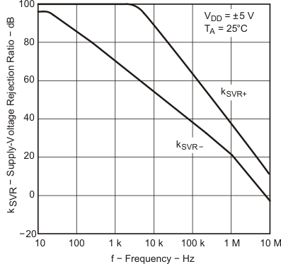
| kSVR | Supply voltage rejection ratio (ΔVDD/ΔVIO) | VDD = 4.4 V to 16 V, | 25°C | 80 | 95 | dB | ||
| VIC = VDD/2, | No load | Full range | 80 | |||||
| IDD | Supply current | VO = 2.5 V, | No load | 25°C | 4.4 | 6 | mA | |
| Full range | 6 | |||||||
(1) Full range is −40°C to 150°C for thisl part.
(2) Typical values are based on the input offset voltage shift observed through 168 hours of operating life test at TA = 150°C extrapolated to TA = 25°C using the Arrhenius equation and assuming an activation energy of 0.96 eV.
(3) Referenced to 2.5 V
6.6 Operating Characteristics, VDD = 5 V
at specified free-air temperature, VDD = 5 V (unless otherwise noted)| PARAMETER | TEST CONDITIONS | TA(1) | MIN | TYP | MAX | UNIT | ||
|---|---|---|---|---|---|---|---|---|
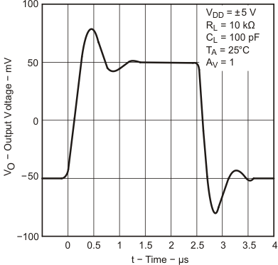
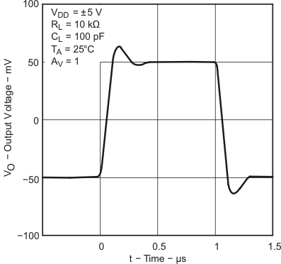
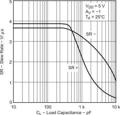
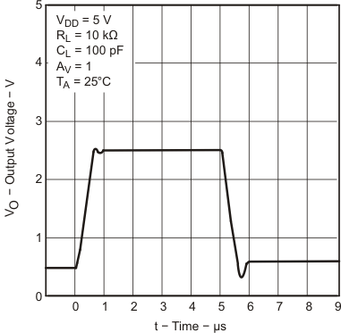
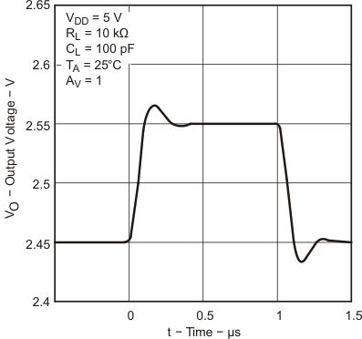
| SR | Slew rate at unity gain | VO = 0.5 V to 2.5 V, CL = 100 pF(2) |
RL = 10 kΩ(2) | 25°C | 2.3 | 3.6 | V/μs | |
| Full range | 1.2 | |||||||
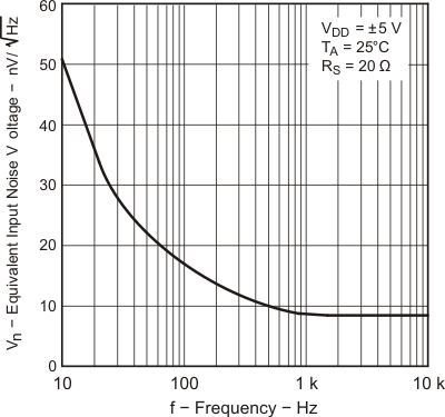
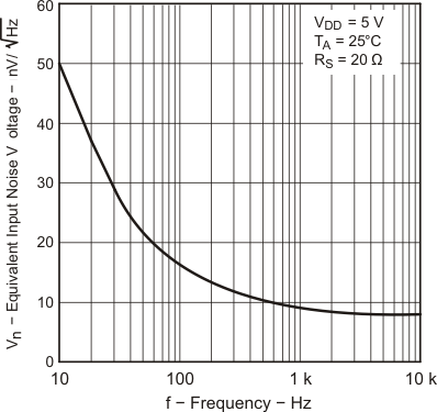
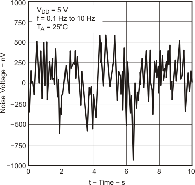
| Vn | Equivalent input noise voltage | f = 10 Hz | 25°C | 50 | nV/√Hz | |||
| f = 1 kHz | 25°C | 9 | ||||||
| VN(pp) | Peak-to-peak equivalent input noise voltage | f = 0.1 to 1 Hz | 25°C | 1 | μV | |||
| f = 0.1 to 10 Hz | 25°C | 1.4 | ||||||
| In | Equivalent input noise current | 25°C | 0.6 | fA/√Hz | ||||
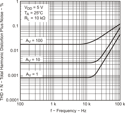
| THD + N | Total harmonic distortion plus noise | VO = 0.5V to 2.5V, RL = 10 kΩ, f = 20 kHz (2) |
AV = 1 | 25°C | 0.0013% | |||
| AV = 10 | 0.004% | |||||||
| AV = 100 | 0.03% | |||||||
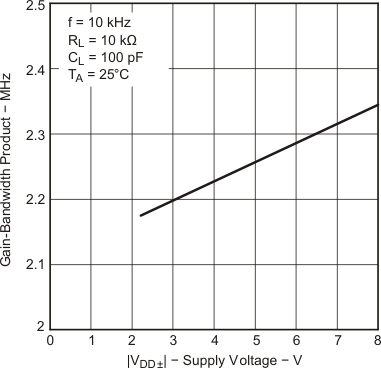
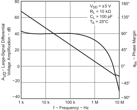
| Gain-bandwidth product | f = 10 kHz, CL = 100 pF(2) |
RL = 10 kΩ(2) | 25°C | 2.18 | MHz | |||
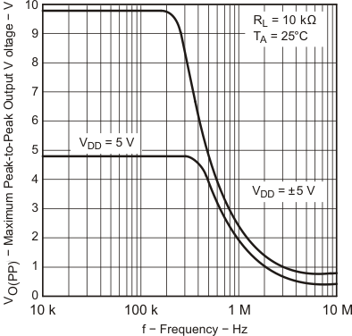
| BOM | Maximum output-swing bandwidth | VO(PP) = 2V, RL = 10 kΩ(2) |
AV = 1, CL = 100 pF(2) |
25°C | 1 | MHz | ||
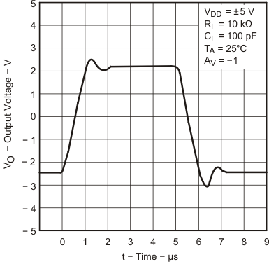
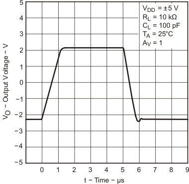
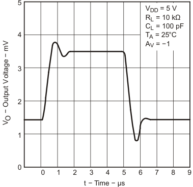
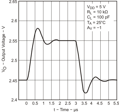
| ts | Settling time | AV = -1, Step = 0.5V to 2.5V, RL = 10 kΩ(2) CL = 100 pF(2) |
To 0.1% | 25°C | 1.5 | μs | ||
| To 0.01% | 2.6 | |||||||
| φm | Phase margin at unity gain | RL = 10 kΩ | CL = 100 pF(2) | 25°C | 50° | |||
| Gain margin | 25°C | 10 | dB | |||||
(1) Full range is −40°C to 150°C for this part.
(2) Referenced to 2.5 V
6.7 Electrical Characteristics, VDD± = ±5 V
at specified free-air temperature, VDD± = ±5 V (unless otherwise noted)| PARAMETER | TEST CONDITIONS | TA(1) | MIN | TYP | MAX | UNIT | ||
|---|---|---|---|---|---|---|---|---|
| VIO | Input offset voltage | VIC = 0 V, RS = 50 Ω |
VO = 0 V | 25°C | 300 | 2500 | μV | |
| Full range | 3000 | |||||||
| αVIO | Temperature coefficient of input offset voltage | 25°C to 125°C | 2 | μV/°C | ||||
| Input offset voltage long-term drift(2) | 25°C | 0.002 | μV/mo | |||||
| IIO | Input offset current | 25°C | 0.5 | 60 | pA | |||
| Full range | 7000 | |||||||
| IIB | Input bias current | 25°C | 1 | 60 | pA | |||
| Full range | 7000 | |||||||
| VICR | Common-mode input voltage range | RS = 50 Ω | |VIO| ≤ 5 mV | 25°C | −5 to 4 | −5.3 to 4.2 | V | |
| Full range | −5 to 3.5 | |||||||
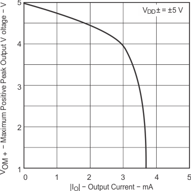
| VOM+ | Maximum positive peak output voltage | IO = −20 μA | 25°C | 4.99 | V | |||
| IO = −200 μA | 25°C | 4.85 | 4.93 | |||||
| Full range | 4.84 | |||||||
| IO = −1 mA | 25°C | 4.25 | 4.65 | |||||
| Full range | 4.20 | |||||||
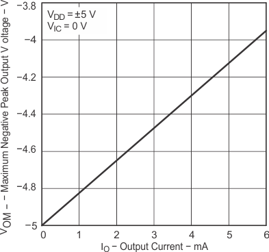
| VOM- | Maximum negative peak output voltage | VIC = 0 V, | IO = 50 μA | 25°C | −4.99 | V | ||
| VIC = 0 V, | IO = 500 μA | 25°C | −4.85 | −4.91 | ||||
| Full range | −4.85 | |||||||
| VIC = 0 V, | IO = 5 mA | 25°C | −3.5 | −4.1 | ||||
| Full range | −3.45 | |||||||
| AVD | Large-signal differential voltage amplification | VO = ±4 V, | RL = 10 kΩ | 25°C | 20 | 50 | V/mV | |
| Full range | 16 | |||||||
| RL = 1 MΩ | 25°C | 300 | ||||||
| rid | Differential input resistance | 25°C | 1012 | Ω | ||||
| ri | Common-mode input resistance | 25°C | 1012 | Ω | ||||
| ci | Common-mode input capacitance | f = 10 kHz, | N package | 25°C | 8 | pF | ||
| zo | Closed-loop output impedance | f = 1 MHz, | AV = 10 | 25°C | 130 | Ω | ||
| CMRR | Common-mode rejection ratio | VIC = -5 V to 2.7 V, VO = 0 V, |
RS = 50 Ω | 25°C | 75 | 80 | dB | |
| Full range | 73 | |||||||
| kSVR | Supply voltage rejection ratio (ΔVDD/ΔVIO) | VDD = ±2.2 V to ±8 V, | 25°C | 80 | 95 | dB | ||
| VIC = 0V, | No load | Full range | 80 | |||||
| IDD | Supply current | VO = 0 V, | No load | 25°C | 4.4 | 6 | mA | |
| Full range | 6 | |||||||
(1) Full range is −40°C to 150°C for this part.
(2) Typical values are based on the input offset voltage shift observed through 168 hours of operating life test at TA = 150°C extrapolated to TA = 25°C using the Arrhenius equation and assuming an activation energy of 0.96 eV.
6.8 Operating Characteristics, VDD± = ±5 V
at specified free-air temperature, VDD± = ±5 V (unless otherwise noted)| PARAMETER | TEST CONDITIONS | TA(1) | MIN | TYP | MAX | UNIT | ||
|---|---|---|---|---|---|---|---|---|
| SR | Slew rate at unity gain | VO = ±2.3 V, RL = 10 kΩ |
CL = 100 pF | 25°C | 2.3 | 3.6 | V/μs | |
| Full range | 1.2 | |||||||
| Vn | Equivalent input noise voltage | f = 10 Hz | 25°C | 50 | nV/√Hz | |||
| f = 1 kHz | 25°C | 9 | ||||||
| VN(pp) | Peak-to-peak equivalent input noise voltage | f = 0.1 to 1 Hz | 25°C | 1 | μV | |||
| f = 0.1 to 10 Hz | 25°C | 1.4 | ||||||
| In | Equivalent input noise current | 25°C | 0.6 | fA/√Hz | ||||
| THD + N | Total harmonic distortion plus noise | VO = ±2.3 V, f = 20 kHz, RL = 10 kΩ |
AV = 1 | 25°C | 0.0011% | |||
| AV = 10 | 0.004% | |||||||
| AV = 100 | 0.03% | |||||||
| Gain-bandwidth product | f = 10 kHz, CL = 100 pF |
RL = 10 kΩ | 25°C | 2.25 | MHz | |||
| BOM | Maximum output-swing bandwidth | VO(PP) = 4.6 V, RL = 10 kΩ |
AV = 1, CL = 100 pF |
25°C | 0.54 | MHz | ||
| ts | Settling time | AV = -1, Step = -2.3 V to 2.3 V, RL = 10 kΩ CL = 100 pF |
To 0.1% | 25°C | 1.5 | μs | ||
| To 0.01% | 3.2 | |||||||
| φm | Phase margin at unity gain | RL = 10 kΩ, | CL = 100 pF | 25°C | 52° | |||
| Gain margin | 25°C | 10 | dB | |||||
(1) Full range is −40°C to 150°C for this part.
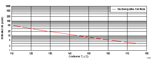
A. See data sheet for Absolute Maximum Ratings and minimum Recommended Operating Conditions.
B. Silicon operating life design goal is 10 years at 105°C junction temperature (does not include package interconnect life).
Figure 2. TLC2274EPWRQ1 Operating Life Derating Chart
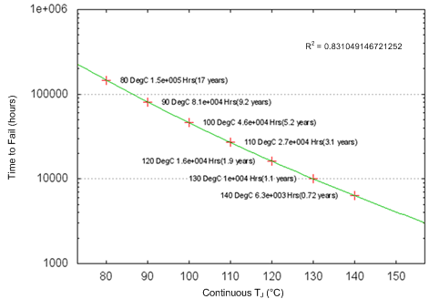 Figure 3. Estimated Wire Bond Life
6.9 Typical Characteristics
Data at high and low temperatures are applicable only within the rated operating free-air temperature ranges of the devices.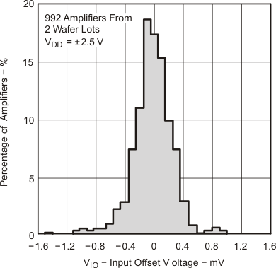
| TA = 25°C |
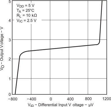
| VDD = ±5 V | VIC = 2.5 V | VO = ±4 V |
| RL = 10 kΩ |
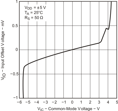
| TA = 25°C |
| TA = 25°C |
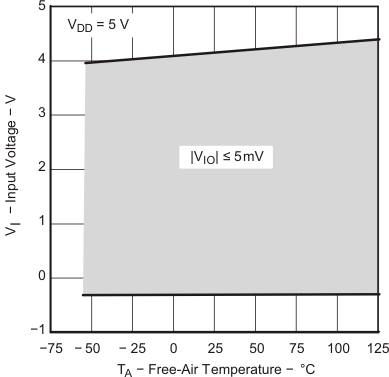
| TA = 25°C |
| VDD = 5 V | VIC = 2.5 V | VO = 1 to 4 V |
| RL = 10 kΩ |
| VDD± = ±2.2 to ±8 V | VO = 0 V |
| VDD = 5 V | RL = 10 kΩ | CL = 100 pF |
| AV = 1 |