ZHCSP69E August 2009 – May 2022 TCA9535
PRODUCTION DATA
- 1 特性
- 2 应用
- 3 说明
- 4 Revision History
- 5 Pin Configuration and Functions
- 6 Specifications
- 7 Detailed Description
- 8 Application and Implementation
- 9 Power Supply Recommendations
- 10Layout
- 11Device and Documentation Support
- 12Mechanical, Packaging, and Orderable Information
封装选项
机械数据 (封装 | 引脚)
散热焊盘机械数据 (封装 | 引脚)
订购信息
5 Pin Configuration and Functions
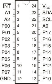
 Figure 5-1 DB, PW (TSSOP) Package
24-Pin (Top View)

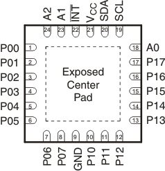
The exposed
center pad, if used, must be connected as a secondary ground or left
electrically open.
Figure 5-2 RTW (WQFN), RGE (VQFN)
Package24-Pin (Top View)
Table 5-1 Pin Functions
| PIN | TYPE | DESCRIPTION | ||
|---|---|---|---|---|
| NAME | NO. | |||
| DB, PW | RTW, RGE | |||
| A0 | 21 | 18 | Input | Address input 0. Connect directly to VCC or ground |
| A1 | 2 | 23 | Input | Address input 1. Connect directly to VCC or ground |
| A2 | 3 | 24 | Input | Address input 2. Connect directly to VCC or ground |
| GND | 12 | 9 | — | Ground |
| INT | 1 | 22 | Output | Interrupt output. Connect to VCC through an external pull-up resistor |
| P00(1) | 4 | 1 | I/O | P-port I/O. Push-pull design structure. At power on, P00 is configured as an input |
| P01(1) | 5 | 2 | I/O | P-port I/O. Push-pull design structure. At power on, P01 is configured as an input |
| P02(1) | 6 | 3 | I/O | P-port I/O. Push-pull design structure. At power on, P02 is configured as an input |
| P03(1) | 7 | 4 | I/O | P-port I/O. Push-pull design structure. At power on, P03 is configured as an input |
| P04(1) | 8 | 5 | I/O | P-port I/O. Push-pull design structure. At power on, P04 is configured as an input |
| P05(1) | 9 | 6 | I/O | P-port I/O. Push-pull design structure. At power on, P05 is configured as an input |
| P06(1) | 10 | 7 | I/O | P-port I/O. Push-pull design structure. At power on, P06 is configured as an input |
| P07(1) | 11 | 8 | I/O | P-port I/O. Push-pull design structure. At power on, P07 is configured as an input |
| P10(1) | 13 | 10 | I/O | P-port I/O. Push-pull design structure. At power on, P10 is configured as an input |
| P11(1) | 14 | 11 | I/O | P-port I/O. Push-pull design structure. At power on, P11 is configured as an input |
| P12(1) | 15 | 12 | I/O | P-port I/O. Push-pull design structure. At power on, P12 is configured as an input |
| P13(1) | 16 | 13 | I/O | P-port I/O. Push-pull design structure. At power on, P13 is configured as an input |
| P14(1) | 17 | 14 | I/O | P-port I/O. Push-pull design structure. At power on, P14 is configured as an input |
| P15(1) | 18 | 15 | I/O | P-port I/O. Push-pull design structure. At power on, P15 is configured as an input |
| P16(1) | 19 | 16 | I/O | P-port I/O. Push-pull design structure. At power on, P16 is configured as an input |
| P17(1) | 20 | 17 | I/O | P-port I/O. Push-pull design structure. At power on, P17 is configured as an input |
| SCL | 22 | 19 | Input | Serial clock bus. Connect to VCC through a pull-up resistor |
| SDA | 23 | 20 | Input | Serial data bus. Connect to VCC through a pull-up resistor |
| VCC | 24 | 21 | — | Supply voltage |
(1) If port is unused, it must be tied to either VCC or
GND through a resistor of moderate value (about 10 kΩ)