ZHCSFV9A May 2016 – December 2016 TAS5722L
PRODUCTION DATA.
- 1 特性
- 2 应用
- 3 说明
- 4 修订历史记录
- 5 Pin Configuration and Functions
- 6 Specifications
-
7 Detailed Description
- 7.1 Overview
- 7.2 Functional Block Diagram
- 7.3 Feature Description
- 7.4 Device Functional Modes
- 7.5
Register Maps
- 7.5.1 I2C Register Map Summary
- 7.5.2
Register Maps
- 7.5.2.1 Device Identification Register (0x00)
- 7.5.2.2 Power Control Register (0x01)
- 7.5.2.3 Digital Control Register 1 (0x02)
- 7.5.2.4 Register Name (offset = ) [reset = ] or (address = ) [reset = ]
- 7.5.2.5 Volume Control Register (0x04)
- 7.5.2.6 Analog Control Register (0x06)
- 7.5.2.7 Fault Configuration and Error Status Register (0x08)
- 7.5.2.8 Digital Clipper 2 Register (0x10)
- 7.5.2.9 Digital Clipper 1 Register (0x11)
- 7.5.2.10 Digital Control Register 3 (0x13)
- 7.5.2.11 Analog Control Register 2 (0x14)
- 8 Applications and Implementation
- 9 Power Supply Recommendations
- 10Layout
- 11器件和文档支持
- 12机械封装和可订购信息
6 Specifications
6.1 Absolute Maximum Ratings
over operating free-air temperature range (unless otherwise noted)(1)| MIN | MAX | UNIT | |||
|---|---|---|---|---|---|
| VCC | Supply voltage(2) | PVDD, AVDD | –0.3 | 20 | V |
| DVDD | –0.3 | 2.25 | |||
| Digital input voltage | Digital inputs referenced to DVDD supply | –0.5 | VDVDD + 0.5 | V | |
| TA | Ambient operating temperature | –25 | 85 | °C | |
| Tstg | Storage temperature range | –40 | 125 | °C | |
(1) Stresses beyond those listed under absolute maximum ratings may cause permanent damage to the device. These are stress ratings only, and functional operation of the device at these or any other conditions beyond those indicated under Recommended Operating Conditions is not implied. Exposure to absolute-maximum-rated conditions for extended periods my affect device reliability.
(2) All voltages are with respect to network ground pin.
6.2 ESD Ratings
| VALUE | UNIT | |||
|---|---|---|---|---|
| V(ESD) | Electrostatic discharge | Human body model (HBM), per ANSI/ESDA/JEDEC JS-001, all pins(1) | ±2000 | V |
| Charged device model (CDM), per JEDEC specification JESD22-C101, all pins(2) | ±750 | |||
(1) JEDEC document JEP155 states that 500-V HBM allows safe manufacturing with a standard ESD control process.
(2) JEDEC document JEP157 states that 250-V CDM allows safe manufacturing with a standard ESD control process.
6.3 Recommended Operating Conditions
over operating free-air temperature range (unless otherwise noted)| MIN | TYP | MAX | UNIT | ||
|---|---|---|---|---|---|
| PVDD AVDD |
Power supply voltage | 4.5 | 17 | V | |
| DVDD | Power supply voltage | 1.65 | 1.8 | 2 | V |
| VIH(DR) | High-level digital input voltage | VDVDD | V | ||
| VIL(DR) | Low-level digital input voltage | 0 | V | ||
| RSPK | Minimum speaker load | 3.2 | Ω | ||
| TA | Operating free-air temperature | –25 | 85 | °C | |
| TJ | Operating junction temperature | –25 | 150 | °C | |
6.4 Thermal Information
| THERMAL METRIC(1) | TAS5722L | UNIT | |
|---|---|---|---|
| RSM (QFN) | |||
| 32 PINS | |||
| RθJA | Junction-to-ambient thermal resistance(2) | 37.3 | °C/W |
| RθJCtop | Junction-to-case (top) thermal resistance(3) | 30.4 | |
| RθJB | Junction-to-board thermal resistance(4) | 7.9 | |
| ψJT | Junction-to-top characterization parameter(5) | 0.4 | |
| ψJB | Junction-to-board characterization parameter(6) | 7.7 | |
| RθJCbot | Junction-to-case (bottom) thermal resistance(7) | 2.5 | |
(1) For more information about traditional and new thermal metrics, see the Semiconductor and IC Package Thermal Metrics application report (SPRA953).
(2) The junction-to-ambient thermal resistance under natural convection is obtained in a simulation on a JEDEC-standard, high-K board, as specified in JESD51-7, in an environment described in JESD51-2a.
(3) The junction-to-case (top) thermal resistance is obtained by simulating a cold plate test on the package top. No specific JEDEC-standard test exists, but a close description can be found in the ANSI SEMI standard G30-88.
(4) The junction-to-board thermal resistance is obtained by simulating in an environment with a ring cold plate fixture to control the PCB temperature, as described in JESD51-8.
(5) The junction-to-top characterization parameter, ψJT, estimates the junction temperature of a device in a real system and is extracted from the simulation data for obtaining RθJA, using a procedure described in JESD51-2a (sections 6 and 7).
(6) The junction-to-board characterization parameter, ψJB, estimates the junction temperature of a device in a real system and is extracted from the simulation data for obtaining RθJA, using a procedure described in JESD51-2a (sections 6 and 7).
(7) The junction-to-case (bottom) thermal resistance is obtained by simulating a cold plate test on the exposed (power) pad. No specific JEDEC standard test exists, but a close description can be found in the ANSI SEMI standard G30-88.
Spacer
Spacer
6.5 Electrical Characteristics
VPVDD = 16.5 V, VDVDD = 1.8 V, RL = 4 Ω + 33 µH, fPWM = 576 kHz, 22-Hz to 20- kHz Bandwidth, AP AUX-0025 + AES17 Filter (unless otherwise noted)| PARAMETER | CONDITIONS | MIN | TYP | MAX | UNIT | |
|---|---|---|---|---|---|---|
| DIGITAL INPUT AND OUTPUT | ||||||
| VIH | High-level digital input logic voltage threshold | All digital pins | 70% | |||
| VIL | Low-level digital input logic voltage threshold | All digital pins | 30% | |||
| IIH | Input logic "high" leakage for digital inputs | All digital pins, excluding SDZ | 15 | µA | ||
| IIL | Input logic "low" leakage for digital inputs | All digital pins, excluding SDZ | –15 | µA | ||
| IIH(SDZ) | Input logic "high" leakage for SDZ inputs | SDZ | 1 | µA | ||
| IIL(SDZ) | Input logic "low" leakage for SDZ inputs | SDZ | –1 | µA | ||
| VOL | Output logic "low" for FAULTZ open drain Output | IOL = –2 mA | 10% VDVDD | |||
| CIN | Input capacitance for digital inputs | All digital pins | 5 | pF | ||
| MASTER CLOCK | ||||||
| DMCLK | Allowable MCLK duty cycle | 45% | 50% | 55% | ||
| fMCLK | MCLK input frequency | 25 | MHz | |||
| Supported single-speed MCLK frequencies | values: 64, 128, 256 and 512 | 2.8 | 24.6 | MHz | ||
| Supported double-speed MCLK frequencies | values: 64, 128 and 256 | 5.6 | 24.6 | MHz | ||
| SERIAL AUDIO PORT | ||||||
| DBCLK | Allowable BCLK duty cycle | 45% | 50% | 55% | ||
| fBCLK | BCLK input frequency | 25 | MHz | |||
| Supported single-speed BCLK frequencies | values: 64, 96, 128, 192 and 256 | 2.8 | 12.3 | MHz | ||
| Supported double-speed BCLK frequencies | values: 64, 96, 128, 192 and 256 | 5.6 | 24.6 | MHz | ||
| fS | Supported single-speed input sample rates | values: 44.1 and 48 | 44.1 | 48 | kHz | |
| Supported double-speed input sample rates | values: 88.2 and 96 | 88.2 | 96 | kHz | ||
| I2C CONTROL PORT | ||||||
| CL(I2C) | Allowable load capacitance for each I2C Line | 400 | pF | |||
| fSCL | SCL frequency | No wait states | 400 | kHz | ||
| PROTECTION | ||||||
| OTETHRESH | Over-temperature error (OTE) threshold | 150 | °C | |||
| OTEHYST | Over-temperature error (OTE) hysteresis | 15 | °C | |||
| OCETHRESH | overcurrent error (OCE) threshold | VPVDD = 16.5 V, TA = 25°C | 5 | A | ||
| DCETHRESH | DC error (DCE) threshold | VPVDD = 16.5V, TA = 25°C | 2.6 | V | ||
| AMPLIFIER PERFORMANCE | ||||||
| POUT | Continuous average power | RL = 8 Ω+33 µH, 1% THD+N, VPVDD = 12 V, fIN = 1 kHz | 8.2 | W | ||
| RL = 8 Ω+33 µH, 1% THD+N, VPVDD = 16.5 V, fIN = 1 kHz | 15.25 | |||||
| RL = 4 Ω+33 µH, 1% THD+N, VPVDD = 12 V, fIN = 1 kHz | 14.25 | |||||
| RL = 4 Ω+33 µH, 1% THD+N, VPVDD = 16.5 V, fIN = 1 kHz | 16 | |||||
| THD+N | Total harmonic distortion plus noise | RL = 8 Ω+33 µH, VPVDD = 12 V, POUT = 4.25 W, 20 Hz ≤ fIN≤ 20 kHz | 0.05% | |||
| RL = 8 Ω+33 µH, VPVDD = 16.5 V, POUT = 4.25 W, 20 Hz ≤ fIN≤ 20 kHz | 0.05% | |||||
| RL = 4 Ω+33 µH, VPVDD = 12 V, POUT = 8.25 W, 20 Hz ≤ fIN≤ 20 kHz | 0.05% | |||||
| RL = 4 Ω+33 µH, VPVDD = 16.5 V, POUT = 8.25 W, 20 Hz ≤ fIN≤ 20 kHz | 0.06% | |||||
| PEFF | Power efficiency | RL = 8 Ω+33 µH, VPVDD = 16.5 V, POUT = 10 W | 90% | |||
| RL = 4 Ω+33 µH, VPVDD = 16.5 V, POUT = 14 W | 87% | |||||
| VN | Integrated noise floor voltage | A-Weighted, Gain = 20.7dBV, RL = 8 Ω+33 µH | 50 | µVrms | ||
| KCP | Click-pop performance | Into and out of HW reset, into and out of SW shutdown, when SAIF clocks are applied or removed and during power rail cycling. Measured using Maxim click-pop measurement method. | -60 | dB | ||
| φ CC | Channel-to-channel phase shift | Output phase shift between multiple devices from 20 Hz to 20 kHz. Across all sample frequencies and SAIF operating modes. | 0.2 | deg | ||
| PSRR | Power supply rejection ratio | AC, 5.5 V ≤ VPVDD ≤ 16.5 V, DVDD = 1.8 V+200 mVP-P, fRIPPLE from 20 Hz to 20 kHz | 69 | dB | ||
| AC, VPVDD = 16.5 V+200 mVP-P, fRIPPLE from 20 Hz to 5 kHz | 64 | |||||
| AC, VPVDD = 16.5 V+100 mVP-P, fRIPPLE from 5 kHz to 20 kHz | 60 | |||||
| AV00 | Amplifier analog gain(1) | ANALOG_GAIN[1:0] register bits set to "00" | 19.2 | dBV | ||
| AV01 | ANALOG_GAIN[1:0] register bits set to "01" | 20.7 | dBV | |||
| AV10 | ANALOG_GAIN[1:0] register bits set to "10" | 23.5 | dBV | |||
| AV11 | ANALOG_GAIN[1:0] register bits set to "11" | 26.3 | dBV | |||
| AVERROR | Amplifier analog gain error | ±0.15 | dB | |||
| VOS | DC output offset voltage | Measured between OUTP and OUTN | 1.5 | mV | ||
| ARIPPLE | Frequency response | Maximum deviation above or below passband gain. | ±0.15 | dB | ||
| fLP | -3 dB Output Cutoff Frequency | 0.47×fS | Hz | |||
| RDS(on)FET | Power stage FET on-resistance | TA = 25°C | 120 | mΩ | ||
| RDS(on)TOT | Power stage total on-resistance (FET+bond+package) | TA = 25°C | 150 | mΩ | ||
| IP-P | Peak output current | TA = 25°C | 5 | A | ||
| fPWM | PWM switching frequency | values: 6, 8, 10, 12, 14, 16, 20 and 24 | 6 | 24 | MHz | |
(1) When PVDD is less than 5.5 V, the voltage regulator that operates the analog circuitry does not have enough headroom to maintain the nominal 5.4-V internal voltage. The lack of headroom causes a direct reduction in gain (approximately –0.8 dB at 5 V and –1.74 dB at 4.5 V), but the device functions properly down to VPVDD = 4.5 V. For operation below 5.5V, the VREG_LVL bit (register 0x14, bit 2) can be set high, which reduces the internal voltage regulator output voltage to prevent variation in gain. When the bit is set high, all gain settings are reduced by 3dB.
6.6 Timing Requirements
| MIN | NOM | MAX | UNIT | |||
|---|---|---|---|---|---|---|
| tACTIVE | Shutdown to Active Time | From deassertion of SDZ (both pin and I2C register bit) until the Class-D amplifier begins switching. | 25 | ms | ||
| tWAKE | Wake Time | From the deassertion of SLEEP until the Class-D amplifier starts switching. | 1 | ms | ||
| tSLEEP | Sleep Time | From the assertion of SLEEP until the Class-D amplifier stops switching. | tvrmp+1 | ms | ||
| tMUTE | Play to Mute Time | From the assertion of MUTE until the volume has ramped to the minimum. | tvrmp | ms | ||
| tPLAY | Un-Mute to Play Time | From the deassertion of MUTE until the volume has returned to its current setting. | tvrmp | ms | ||
| tSD | Active to Shutdown Time | From the assertion of SDZ (pin or I2C register bit) until the Class-D amplifier stops switching. | tvrmp+1 | ms | ||
| SERIAL AUDIO PORT | ||||||
| tH_L | Time High/Low, BCLK, LRCLK, SDI inputs | 10 | ns | |||
| tSU / tHLD | Setup and hold time. LRCLK, SDI input to BCLK edge. | Input tRISE ≤ 1 ns, input tFALL ≤ 1 ns | 5 | ns | ||
| Input tRISE ≤ 4 ns, input tFALL ≤ 4ns | 8 | |||||
| Input tRISE ≤ 8 ns, input tFALL ≤ 8ns | 12 | |||||
| tRISE | Rise-time BCLK, LRCLK, SDI inputs | 8 | ns | |||
| tFALL | Fall-time BCLK, LRCLK, SDI inputs | 8 | ns | |||
| I2C CONTROL PORT | ||||||
| tBUF | Bus free time between start and stop conditions | 1.3 | µs | |||
| tH1(I2C) | Hold Time, SCL to SDA | 0 | ns | |||
| tH2(I2C) | Hold Time, start condition to SCL | 0.6 | µs | |||
| tSTART(I2C) | I2C Startup Time after DVDD Power On Reset | 12 | ms | |||
| tR(I2C) | Rise Time, SCL and SDA | 300 | ns | |||
| tF(I2C) | Fall Time, SCL and SDA | 300 | ns | |||
| tSU1(I2C) | Setup, SDA to SCL | 100 | ns | |||
| tSU2(I2C) | Setup, SCL to start condition | 0.6 | µs | |||
| tSU3(I2C) | Setup, SCL to stop condition | 0.6 | µs | |||
| tW(H) | Required pulse duration, SCL "HIGH" | 0.6 | µs | |||
| tW(L) | Required pulse duration, SCL "LOW" | 1.3 | µs | |||
| PROTECTION | ||||||
| tFAULTZ | Amplifier fault time-out period | DC detect error | 650 | ms | ||
| OTE or OCE fault | 1.3 | s | ||||
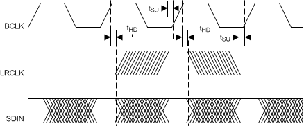 Figure 1. SAIF Timing
 Figure 2. SCL and SDA Timing
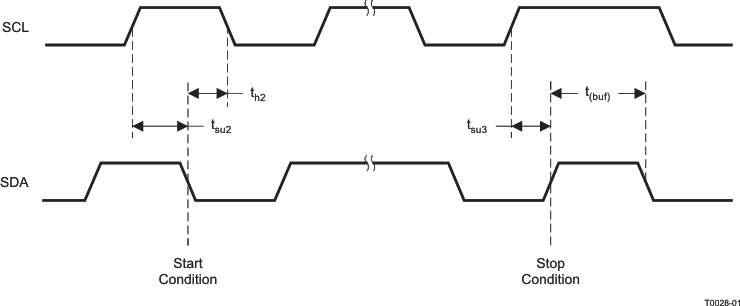 Figure 3. Start and Stop Conditions Timing
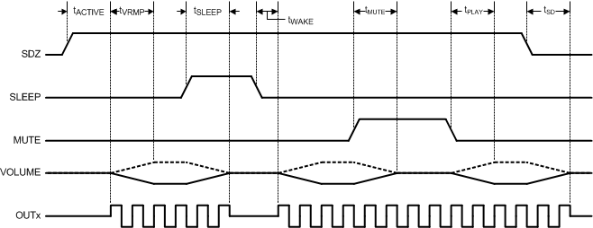 Figure 4. Mode Timing
6.7 Typical Characteristics
TA = 25ºC, VDVDD = 1.8 V, fIN = 1 kHz, fPWM 768 kHz, fs = 48 kHz, Gain = 20.7 dBV, SDZ = 1, Measured using TAS5722LEVM with an Audio Precision SYS-2722 and AUX-0025 filter with 22-Hz-to-20- kHz un-weighted bandwidth using the 20- kHz pre-analyzer filter + 20- kHz brick-wall filter (unless otherwise specified). 33 µH inductors were added in series with 4 Ω loads and 68 µH inductors were placed in series with 8 Ω loads due to the ferrite bead filters.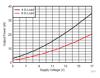
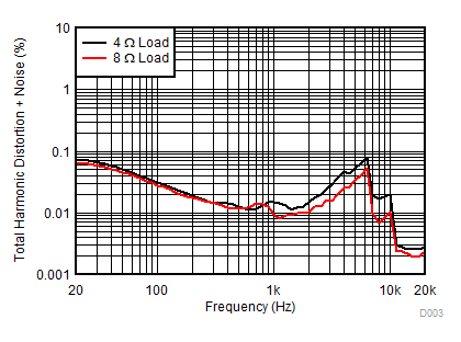
| PVDD = 5 V | Gain = 19.2 dBV | fPWM = 768 kHz |
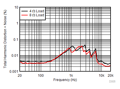
| PVDD = 12 V | Gain = 19.2 dBV | fPWM = 768 kHz |
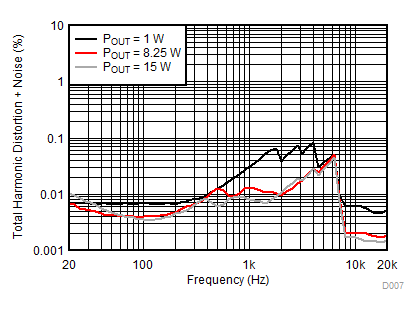
| PVDD = 16.5 V | Gain = 23.5 dBV | RLoad = 4 Ω |
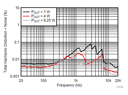
| PVDD = 16.5 V | Gain = 23.5 dBV | RLoad = 8 Ω |
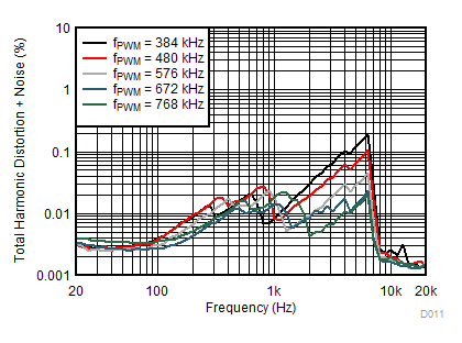
| PVDD = 16.5 V | Gain = 20.7 dBV | POUT = 4.25 W |
| RLoad = 8 Ω |
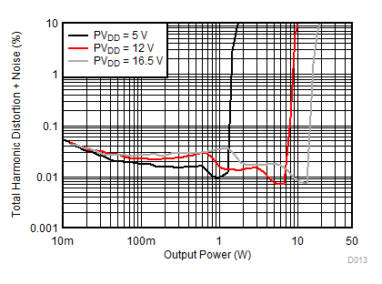
| RLoad = 8 Ω | Gain = 23.5 dBV | fPWM = 768 kHz |
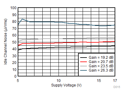
| RLoad = 4 Ω | A-weighting Filter | fPWM = 768 kHz |
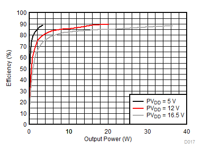
| RLoad = 4 Ω | Gain = 23.5 dBV | fPWM = 768 kHz |
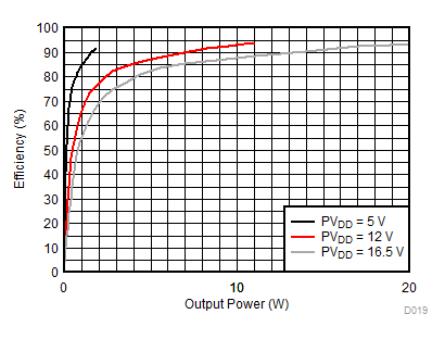
| RLoad = 8 Ω | Gain = 23.5 dBV | fPWM = 768 kHz |
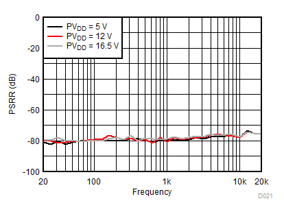
| RLoad = 4 Ω | Gain = 20.7 dBV | fPWM = 768 kHz |
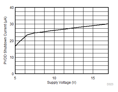
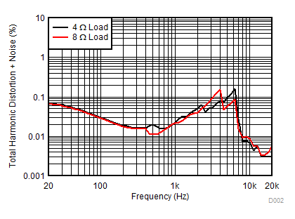
| PVDD = 5 V | Gain = 19.2 dBV | fPWM = 384 kHz |
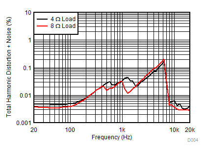
| PVDD = 12 V | Gain = 19.2 dBV | fPWM= 384 kHz |
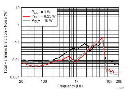
| PVDD = 16.5 V | Gain = 23.5 dBV | fPWM = 384 kHz |
| RLoad = 4 Ω |
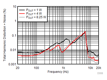
| PVDD = 16.5 V | Gain = 23.5 dBV | fPWM = 384 kHz |
| RLoad = 8 Ω |
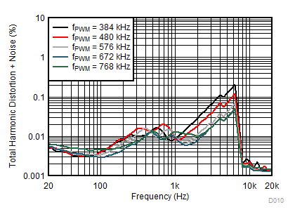
| PVDD = 16.5 V | RLoad = 4 Ω | POUT = 8.25 W |
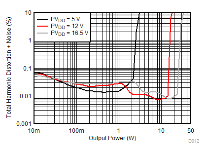
| RLoad = 4 Ω | Gain = 23.5 dBV | fPWM = 768 kHz |
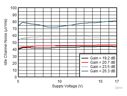
| RLoad = 4 Ω | A-weighting Filter | fPWM = 384 kHz |
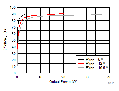
| RLoad = 4 Ω | Gain = 23.5 dBV | fPWM = 384 kHz |
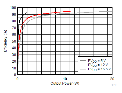
| RLoad = 8 Ω | Gain = 23.5 dBV | fPWM = 384 kHz |
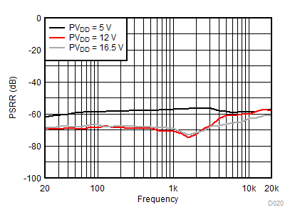
| RLoad = 4 Ω | Gain = 20.7 dBV | fPWM = 768 kHz |
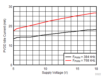
| RLoad = 4 Ω | Gain = 20.7 dBV |