ZHCSCN7C March 2014 – January 2015 TAS5421-Q1
PRODUCTION DATA.
- 1 特性
- 2 应用
- 3 说明
- 4 修订历史记录
- 5 Pin Configuration and Functions
- 6 Specifications
- 7 Detailed Description
- 8 Application and Implementation
- 9 Power Supply Recommendations
- 10Layout
- 11器件和文档支持
- 12机械、封装和可订购信息
10 Layout
10.1 Layout Guidelines
The EVM layout optimizes for thermal dissipation and EMC performance. The TAS5421-Q1 device has a thermal pad down, and good thermal conduction and dissipation require adequate copper area. Layout also affects EMC performance. TAS5421Q1EVM illustrations form the basis for the layout discussions.
10.2 Layout Examples
10.2.1 Top Layer
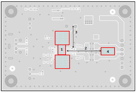
The red boxes around number 1 are the copper ground on the top layer. Soldered directly to the thermal pad, this ground is the first significant thermal dissipation needed. There are vias that go to the other layers for further thermal relief, but vias have high thermal resistance. TI recommends that use of this top layer be mostly for thermal dissipation. A further recommendation is short routes from output pins to the second-order LC filter for EMC suppression. The number 2 arrow indicates these short routes. The shorter the distance, the less EMC radiates. A short route from the PVDD pin to the LC filter from the battery or power source, as indicated by the number 3 arrow, also improves EMC suppression. The red box around number 4 indicates the ground plane that is common to both OUTP and OUTN. Place the capacitors of the LC filter in this common ground plane to help with common-mode noise and short ground loops.
 Figure 18. Top Layer
10.2.2 Second Layer – Signal Layer
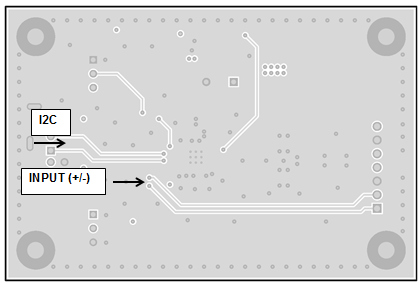
If possible, route the I2C and the positive and negative input traces close together and cover with ground plane, keeping the signals from noise.
 Figure 19. Signal Layer
10.2.3 Third Layer – Power Layer
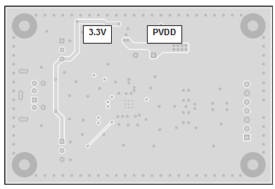
There is no need for a power plane, but TI recommends a wide single PVDD trace to keep the switching noise to a minimum and provide enough current to the device. The wide trace provides a low-impedance path from the power source to the PVDD pin and from the GND pin to the source return. Suppression of switching noise (ripple voltage) on both the positive and return (ground) paths requires a low impedance.
 Figure 20. Power Layer
10.2.4 Bottom Layer – Ground Layer
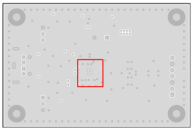
The device has an exposed thermal pad on the bottom side for improved thermal performance. Conducting heat from the thermal pad to other layers requires thermal vias. Because the bottom layer is the secondary heat exchange surface to ambient, the thermal vias area must have low thermal resistance, that is, no signal vias or traces that can increase thermal resistance from the thermal vias to the bottom copper.
 Figure 21. Bottom Layer