SLLS980E June 2009 – November 2016 SN75LVDS83A
PRODUCTION DATA.
- 1 Features
- 2 Applications
- 3 Description
- 4 Revision History
- 5 Description (continued)
- 6 Pin Configuration and Functions
- 7 Specifications
- 8 Parameter Measurement Information
- 9 Detailed Description
- 10Application and Implementation
- 11Power Supply Recommendations
- 12Layout
- 13Device and Documentation Support
- 14Mechanical, Packaging, and Orderable Information
9 Detailed Description
9.1 Overview
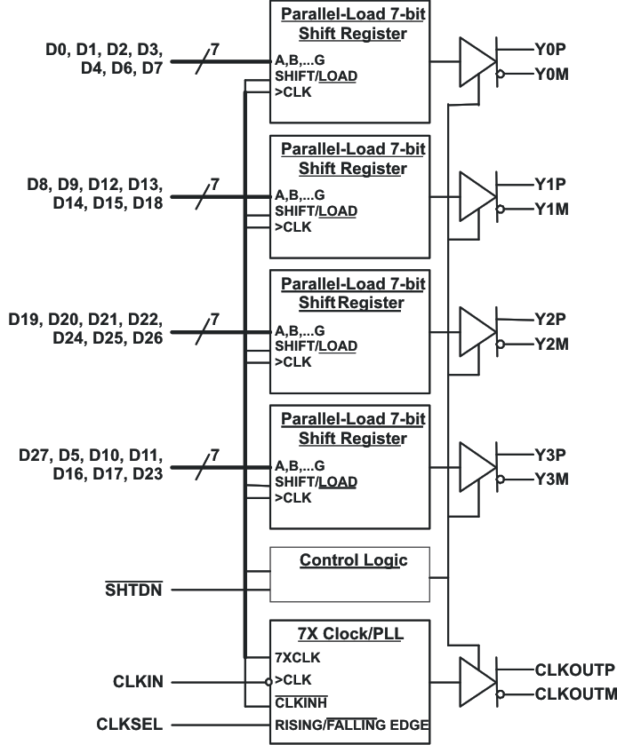
The Flatlink™ is a LVDS SerDes data transmission system. The SN75LVDS83A device takes in three (or four) data words each containing seven single-ended data bits and converts this to an LVDS serial output. Each serial output runs at seven times that of the parallel data rate. The deserializer (receiver) device operates in the reverse manner. The three (or four) LVDS serial inputs are transformed back to the original seven-bit parallel single-ended data. Flatlink™ devices are available in 21:3 or 28:4 SerDes ratios.
The 21-bit devices are designed for 6-bit RGB video for a total of 18 bits in addition to three extra bits for horizontal synchronization, vertical synchronization, and data enable. The 28-bit devices are intended for 8-bit RGB video applications. Again, the extra four bits are for horizontal synchronization, vertical synchronization, data enable, and the remaining is the reserved bit. These 28-bit devices can also be used in 6-bit and 4-bit RGB applications as shown in the subsequent system diagrams.
9.2 Functional Block Diagram

9.3 Feature Description
9.3.1 TTL Input Data
The data inputs to the transmitter come from the graphics processor and consist of up to 24 bits of video information, a horizontal synchronization bit, a vertical synchronization bit, an enable bit, and a spare bit.
The data can be loaded into the registers upon either the rising or falling edge of the input clock selectable by the CLKSEL pin. Data inputs are 1.8 V to 3.3 V tolerant for the SN75LVDS83A and can connect directly to low-power, low-voltage application and graphic processors. The bit mapping is listed in Table 1.
Table 1. Pixel Bit Ordering
| RED | GREEN | BLUE | |
|---|---|---|---|
| LSB | R0 | G0 | B0 |
| R1 | G1 | B1 | |
| R2 | G2 | B2 | |
| 4-bit MSB | R3 | G3 | B3 |
| R4 | G4 | B4 | |
| 6-bit MSB | R5 | G5 | B5 |
| R6 | G6 | B6 | |
| 8-bit MSB | R7 | G7 | B7 |
9.3.2 LVDS Output Data
The pixel data assignment is listed in Table 2 for 24-bit, 18-bit, and 12-bit color hosts.
Table 2. Pixel Data Assignment
| SERIAL CHANNEL | DATA BITS | 8-BIT | 6-BIT | 4-BIT | |||
|---|---|---|---|---|---|---|---|
| FORMAT-1(1) | FORMAT-2(2) | FORMAT-3(3) | NON-LINEAR STEP SIZE(4) | LINEAR STEP SIZE(5) | |||
| Y0 | D0 | R0 | R2 | R2 | R0 | R2 | VCC |
| D1 | R1 | R3 | R3 | R1 | R3 | GND | |
| D2 | R2 | R4 | R4 | R2 | R0 | R0 | |
| D3 | R3 | R5 | R5 | R3 | R1 | R1 | |
| D4 | R4 | R6 | R6 | R4 | R2 | R2 | |
| D6 | R5 | R7 | R7 | R5 | R3 | R3 | |
| D7 | G0 | G2 | G2 | G0 | G2 | VCC | |
| Y1 | D8 | G1 | G3 | G3 | G1 | G3 | GND |
| D9 | G2 | G4 | G4 | G2 | G0 | G0 | |
| D12 | G3 | G5 | G5 | G3 | G1 | G1 | |
| D13 | G4 | G6 | G6 | G4 | G2 | G2 | |
| D14 | G5 | G7 | G7 | G5 | G3 | G3 | |
| D15 | B0 | B2 | B2 | B0 | B2 | VCC | |
| D18 | B1 | B3 | B3 | B1 | B3 | GND | |
| Y2 | D19 | B2 | B4 | B4 | B2 | B0 | B0 |
| D20 | B3 | B5 | B5 | B3 | B1 | B1 | |
| D21 | B4 | B6 | B6 | B4 | B2 | B2 | |
| D22 | B5 | B7 | B7 | B5 | B3 | B3 | |
| D24 | HSYNC | HSYNC | HSYNC | HSYNC | HSYNC | HSYNC | |
| D25 | VSYNC | VSYNC | VSYNC | VSYNC | VSYNC | VSYNC | |
| D26 | ENABLE | ENABLE | ENABLE | ENABLE | ENABLE | ENABLE | |
| Y3 | D27 | R6 | R0 | GND | GND | GND | GND |
| D5 | R7 | R1 | GND | GND | GND | GND | |
| D10 | G6 | G0 | GND | GND | GND | GND | |
| D11 | G7 | G1 | GND | GND | GND | GND | |
| D16 | B6 | B0 | GND | GND | GND | GND | |
| D17 | B7 | B1 | GND | GND | GND | GND | |
| D23 | RSVD | RSVD | GND | GND | GND | GND | |
| CLKOUT | CLKIN | CLK | CLK | CLK | CLK | CLK | CLK |
9.4 Device Functional Modes
9.4.1 Input Clock Edge
The transmission of data bits D0 through D27 occurs as each are loaded into registers upon the edge of the CLKIN signal, where the rising or falling edge of the clock may be selected through CLKSEL. The selection of a clock rising edge occurs by inputting a high level to CLKSEL, which is achieved by populating pullup resistor to pull CLKSEL is high. Inputting a low level to select a clock falling edge is achieved by directly connecting CLKSEL to GND.
9.4.2 Low Power Mode
The SN75LVDS83A can be put in low-power consumption mode by active-low input SHTDN#.
Connecting terminal SHTDN to GND inhibits the clock and shut off the LVDS output drivers for lower power consumption. A low level on this signal clears all internal registers to a low level.
Populate a pullup to VCC on SHTDN# to enable the device for normal operation.
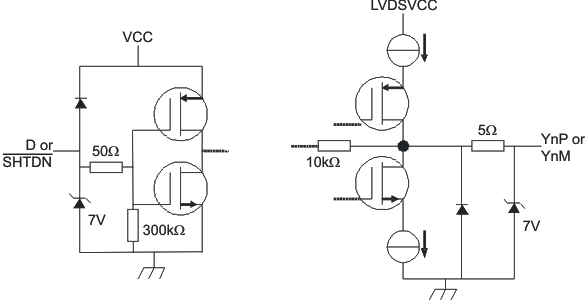
 Figure 13. Equivalent Input and Output Schematic Diagrams