SLLSE41H June 2010 – March 2016 SN75LVCP601
PRODUCTION DATA.
- 1 Features
- 2 Applications
- 3 Description
- 4 Revision History
- 5 Pin Configuration and Functions
- 6 Specifications
- 7 Parameter Measurement Information
- 8 Detailed Description
- 9 Application and Implementation
- 10Power Supply Recommendations
- 11Layout
- 12Device and Documentation Support
- 13Mechanical, Packaging, and Orderable Information
8 Detailed Description
8.1 Overview
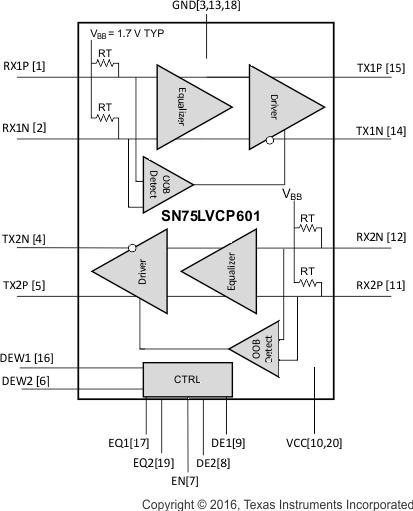
The SN75LVCP601 device is a dual-channel, single-lane SATA redriver and signal conditioner supporting data rates up to 6 Gbps.
This device complies with SATA physical link 2m and 3i specifications. The SN75LVCP601 device is designed to handle interconnect losses at both its input and output. The input stage of each channel offers selectable equalization settings that can be programmed to match the loss of the channel. The outputs provide selectable de-emphasis to compensate for the distortion the SATA signal is expected to experience. The level of equalization and de-emphasis settings depend on the length of interconnect and it’s characteristics. Equalization for input trace and output trace are individually controlled by the setting of EQ1 and EQ2. De-emphasis levels for input and output trace are individually controlled by the setting of DE1, DE2, DEW1 and DEW2 pins.
8.2 Functional Block Diagram
 Figure 25. Data Flow Block Diagram
8.3 Feature Description
8.3.1 Input Equalization
Each differential input of the SN75LVCP601 device has programmable equalization in its front stage. Table 1 lists the equalization. The input equalizer design recovers a signal even when no eye is present at the receiver, and effectively supports FR4 trace at the input anywhere from 4 in. (10.2 cm) to 20 in. (50.8 cm) at SATA 6G speed.
8.3.2 Output De-Emphasis
The SN75LVCP601 device provides the de-emphasis settings shown in Table 1. De-emphasis control is independent for each channel, controlled by the DE1 and DE2 pin settings as shown in Table 1. The reference for the de-emphasis settings available in the device is the transition bit amplitude for each given configuration; this transition bit amplitude is different at 0 dB than the –2-dB and –4-dB settings by design. DEW1 and DEW2 control the DE durations for channels one and two, respectively. Table 1 lists the recommended settings for these control pins. Output de-emphasis is capable of supporting FR4 trace at the output anywhere from
2 in. (5.1 cm) to 12 in. (30.5 cm) at SATA 3G/6G speed.
Table 1. TX and RX EQ and DE Pulse-Duration Settings
8.3.3 Out-of-Band (OOB) Support
The squelch detector circuit within the device enables full detection of OOB signaling as specified in the SATA specification. The device does not detect differential signal amplitude at the receiver input of 50 mVpp or less an activity, and hence does not passed it to the output. The device detects differential signal amplitude of
150 mVp-p or more as an activity and therefore passes it to the output, providing an indication of the activity. Squelch circuit ON or OFF time is 5 ns, maximum. While in squelch mode, outputs are held to VCM.
8.4 Device Functional Modes
8.4.1 Low-Power Mode
There are two low-power modes supported by the SN75LVCP601 device, listed as follows:
- Standby mode (triggered by the EN pin, EN = 0 V)
- The enable (EN) pin controls th low-power mode. Pulling this pin LOW puts the device in standby mode within 2 µs (max). In this mode, the device drives all its active components to their quiescent level, and differential outputs Hi-Z (open). Maximum power dissipation in this mode is 5 mW. Exiting from this mode to normal operation requires a maximum latency of 5 µs.
- Auto low-power mode (triggered when a given channel is in the electrically idle state for more than 100 µs and EN = VCC)
- The device enters and exits low-power mode by actively monitoring the input signal (VIDp-p) level on each of its channels independently. When the input signal on either or both channels is in the electrically idle state, that is, VIDp-p < 50 mV and stays in this state for >100 µs, the associated channel enters into the low-power state. In this state, output of the associated channel goes to VCM and the device selectively shuts off some circuitry to lower power by >80% of its normal operating power. Exit time from the auto low-power mode is <50 ns.