SLLS977F April 2009 – July 2017 SN75DP139
PRODUCTION DATA.
- 1 Features
- 2 Applications
- 3 Description
- 4 Revision History
- 5 Pin Configuration and Functions
-
6 Specifications
- 6.1 Absolute Maximum Ratings
- 6.2 ESD Ratings
- 6.3 Recommended Operating Conditions
- 6.4 Thermal Information
- 6.5 Electrical Characteristics (Device Power)
- 6.6 Electrical Characteristics (Hot Plug Detect)
- 6.7 Electrical Characteristics (Aux / I2C Pins)
- 6.8 Electrical Characteristics (TMDS and Main Link Pins)
- 6.9 Switching Characteristics (Hot Plug Detect)
- 6.10 Switching Characteristics (Aux / I2C Pins)
- 6.11 Switching Characteristics (TMDS and Main Link Pins)
- 6.12 Typical Characteristics
- 7 Detailed Description
- 8 Application and Implementation
- 9 Power Supply Recommendations
- 10Layout
- 11Device and Documentation Support
- 12Mechanical, Packaging, and Orderable Information
封装选项
机械数据 (封装 | 引脚)
散热焊盘机械数据 (封装 | 引脚)
订购信息
8 Application and Implementation
NOTE
Information in the following applications sections is not part of the TI component specification, and TI does not warrant its accuracy or completeness. TI’s customers are responsible for determining suitability of components for their purposes. Customers should validate and test their design implementation to confirm system functionality.
8.1 Application Information
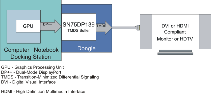
The typical application for the SN75DP139 is to translate from DP++ to TMDS, and thus expand the connectivity for any DP++ source to HDMI 1.4b and DVI sinks. This can be clearly explained when you have the SN75DP139 in a dongle connected to the DP++ source.
8.2 Typical Application
 Figure 32. Typical Application
8.2.1 Design Requirements
| DESIGN PARAMETERS | VALUE |
|---|---|
| VDD Main Power Supply | 3.0 - 3.6 V |
| Main Link Peak-to-Peak AC Input Differential Voltage | 0.15 - 1.2 V |
| TMDS Output Termination Voltage | 3.0 - 3.6 V |
| TMDS Output Swing Voltage Bias Resistor | 3.65 - 4.02 kΩ |
8.2.2 Detailed Design Procedure
8.2.2.1 DVI Application
In DVI application case, it is recommended that between the SN75DP139 TMDS outputs (OUT_Dx) and a through hole DVI connector that a series resistor placeholder is incorporated. This could help in case if there are signal integrity issues as well as help pass system level compliance.
8.2.3 Application Curve
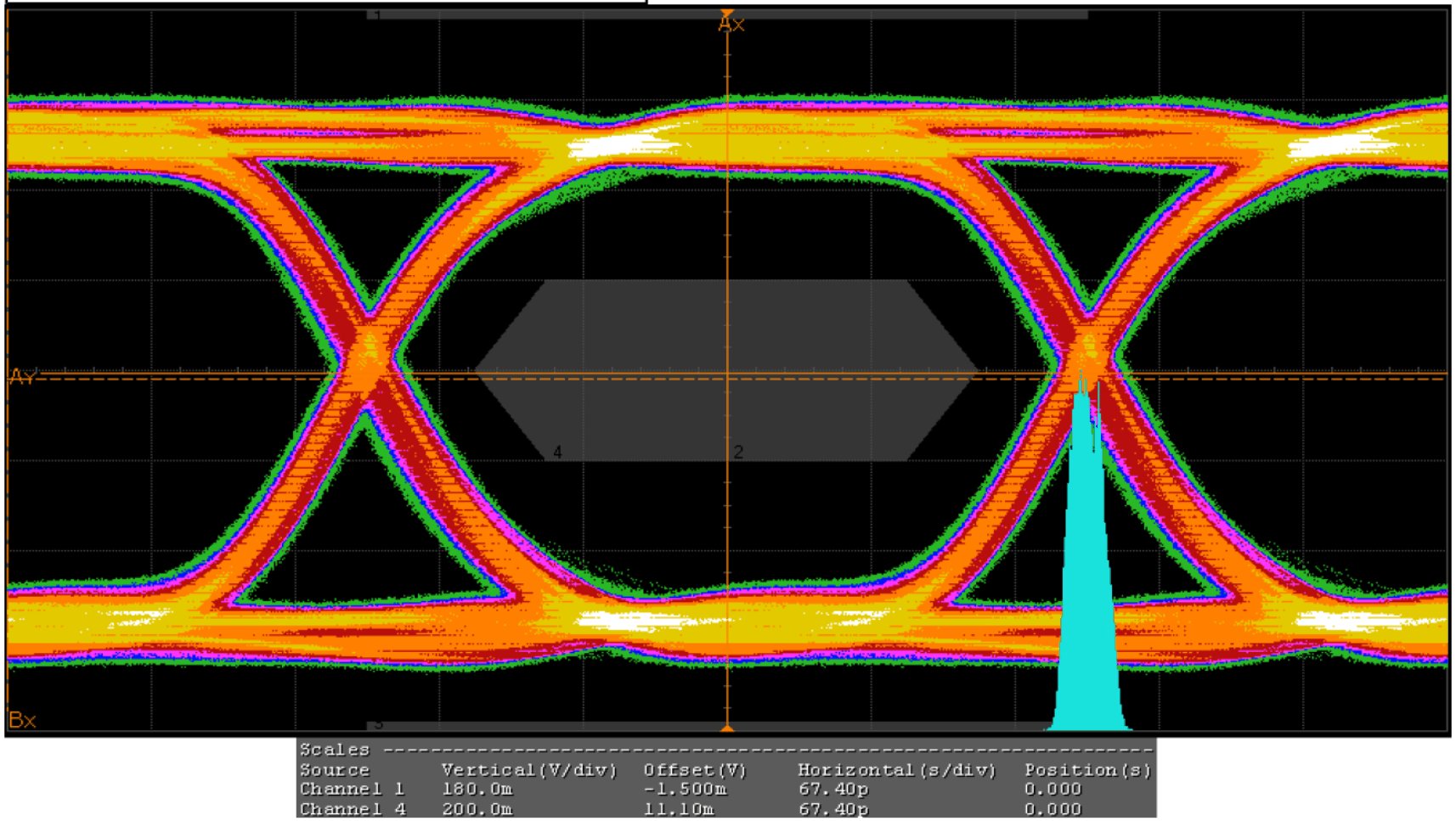
 Figure 33. Data Jitter